

Impedance controlled PCBs
Impedance controlled PCBs
1.Introduction
Impedance Controlled PCBs are fabricated with tightly controlled dimensional tolerances to ensure the PCBs have signal transmission lines with accurate impedances. Upon request, Hopetimepcb offers free of charge design stack-up and impedance calculation assistance to help clients design Impedance Controlled PCBs. In the conceptual level of your PCB design, our team is willing to work with your engineering team to better control impedance by selecting the proper material and stack up.
Electrical impedance is the total amount of opposition given to the electrical current flow in an electrical circuit. Impedance can be calculated using the resistance and reactance of the current in a circuit when a voltage is applied measured and expressed in ohms. Resistance is the opposition to an electrical current flow present in all materials. Reactance is the opposition to an electrical current flow from inherent capacitance and inductance in the electrical circuit interacting with changes in the voltage and current.
Theoretically, for an ideal PCB performance situation, all output energy from a component’s output pin would flow through the connected PCB routing into the load input pin on the other end. However, in reality, not all the energy is absorbed by the load, and any leftover energy would be reflected back into the PCB routing, flowing back toward the output source pin. Reflected energy is a concern for AC (Alternating Current) signals because reflected energy can cause noise that interferes with the original signal, changing the signal’s waveform. In the worst-case scenario, reflected energy would affect the signal’s integrity, resulting in unpredictable PCB behaviour. Impedance matching is not as much of a concern for Digital DC (Direct Current) signals as signals are either high or low, and devices’ noise thresholds are usually able to compensate for the small amount of noise from reflected energy.
Energy being reflected back and forth between the source and the load in a PCB can be avoided by impedance matching. In theory, matching impedance should ensure all of the energy emitted from the source flows into the load with little to no reflected energy.
For a PBC to be considered to have controlled impedance, the routing of the traces must be designed in such a way that the impedance matches the specifications. In order to control impedance in a PCB, both the components and traces of the board must be matched correctly.Hopetimepcb strives to keep standard PCB materials in stock at all times, including:
• Higher copper weights: 2 oz., 3 oz.; heavier weights (WithLead Time)
• Odd copper weights: H/1 oz., H/2 oz., 1/2 oz.
• Foil: 1/4 oz., H oz., 1 oz., 2 oz., 3 oz.
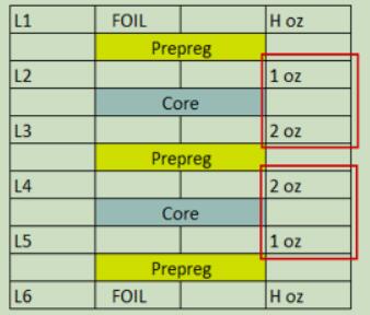 Figure 1:Sample Impedance Control Stackup
2. Impedance Controlled PCB Types
There are two types of Impedance Controlled PCBs, Foil-built, and Core-built. We offer Foil-built PCBs as a default choice since it is more economical and is slightly easier to process. Foil-built PCB consists of one less core layer than core-built PCBs, as shown in the stack-up (Table 1) below,with copper foil layers on the outside. Foil-built boards require various types of foils with different copper weights. However, foils are much easier to acquire than different types of cores. Another factor to consider is that since Foil-built PCBs are covered in copper foil, the designer has more choice in regards to dielectric thickness for the outer layers due to using prepreg. Using prepreg boards is less expensive compared to cores,especially if the core is 5 Mils or thinner.
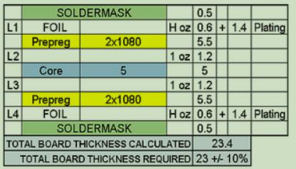 Table 1:Foil Build
A Core-built PCB would have core layers on the outside, so there is no need to use copper foil layers. However, material availability depends on the market, so cores with uneven copper weights may be difficult to acquire. In that case, PCB manufacturers need to order cores with higher copper weight then etch down the cores,which is costly since additional labour costs are involved. Using cores with higher copper weight also adds to the material cost.
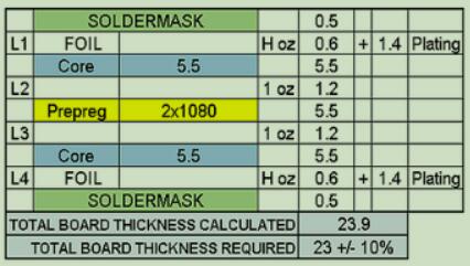 Table 2:Core Build
3.Impedance Calculators
Impedance calculators are computer programs with many different sub-programs assembled together to simulate the expected performance of transmission lines and PCB materials. Impedance calculations have many complicated formulas, and the more complicated the PCB design is, the more complicated the formulas will be. Thus, impedance calculators require a skilled user who knows how to use these programs effectively and the underlying theory.Hopetimepcb will provide free impedance calculations for PCB designs upon request . For performing impedance calculations, we at Hopetimepcb use the industry-standard Polar Impedance Calculator SI8000 or SI9000. We enter published prepreg values from datasheets and your specific design parameters onto the Impedance Calculator to calculate the impedance of PCB design.
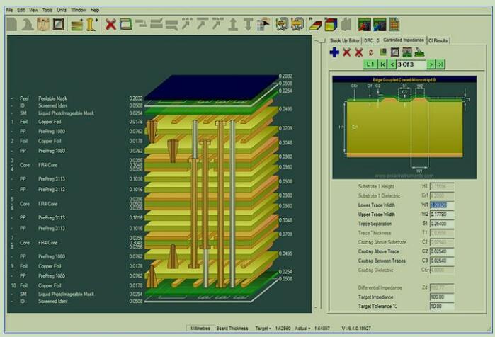
Figure 2:Impedance Calculator Software
4.Impedance Models
Impedance Models are diagrams with symbols labelled and showing the parameters for impedance calculation.We at Hopetimepcb offer to provide these Impedance Model diagrams with impedance parameters.
5.Impedance Affect Stack-up
Stack-Up is the number and arrangement of different layers in a PCB design. Stack-up design choices and parameters are affected by many factors (such as impedance, physical structure, blind holes and so on). Stack up structure features affect the impedance on your signal lines. Changing the stack-up parameters can help to achieve your desired impedance, however, there may be other factors in your design that affect the stack-up to consider and balance. Some relationships to consider are listed below.
•The thicker the dielectric thickness is, the higher the impedance value will be.
•The smaller the dielectric constant is, the greater the impedance value will be.
•The thicker the copper weight is, the lower the impedance value will be.
•A thinner impedance trace width means a higher impedance value.
•Greater Inductance means higher impedance.
•Greater Capacitance means lower impedance.
For microstrip and stripline transmission lines, the largest factors that affect the impedance of a line are the dielectric constant of the substrate, the thickness of the copper and the width of the line. Our dielectric constants are listed in Material Selection & Properties. Please inquire about our available Rogers RF substrates if desired. Next, you may select your desired copper weight. With these two factors chosen, our impedance calculations can aid you in determining the width of your transmission lines.
6.Hopetimepcb TDR Calculations
TDR is “Time Domain Reflectometry” is a measurement technique for determining the characteristics of electrical lines in a PCB by observing reflected waveforms. TDR can also refer to a Time Domain Reflectometer,a type of electronic instrument needed to use time-domain reflectometry to analyze electrical or optical transmission media such as coaxial cable and optical fibre. For example, we can use TDR on a twisted pair wire or coaxial cable to locate faults and discontinuities in wire connection and other transmission media.Hopetimepcb can use Time Domain Reflectometry (TDR) as a way to test whether impedance in a PCB is matched or not. However, our factory usually uses a different machine to test. A TDR test is performed by applying a very fast electrical step signal to the PCB using a controlled impedance cable and probe. The TDR testing equipment records and graphs the changes in impedance value using the part of the signal, which is reflected back. This graph data shows the impedance values for that PCB or the values simulated by the TDR test with average, standard deviation, minimum and maximum values.
7.TDR Coupons
A TDR coupon is a type of small test board on which we can perform impedance testing to verify if the board’s impedance matches your request. Testing the impedance trace in a PCB after fabricating is difficult, and the board may be scrapped due to the fixture. Thus, to replace PCB impedance testing, we provide a TDR coupon for simulating the board traces to test the impedance of the PCB. On the TDR coupon, we will include specifications of the impedance value, trace width and expected dimensions of the PCB so that test results of the TDR coupon should match.Hopetimepcb will provide serialized TDR coupons for each batch of PCB free of charge with our impedance report. If we have a PCB order with 2000 PCBs, of which we build one batch of 1000 pieces first,then build the rest a few days later,then we provide two coupons, one for each batch. The TDR coupon for each batch of PCB are fabricated at the same time as when fabricating the boards. Each coupon is built at the same time as PCB fabrication to ensure that they match your PCB,this way , we provide a TDR coupon to you for impedance testing of each batch.
Click here to know more:What is the difference between Controlled Dielectric and Controlled Impedance regarding PCB fabrication?
Click here to know more:How to control PCB impedance in design?
Back to the Technology Data
PCB Blog
Contact Us
E-mail: [email protected]
E-mail: [email protected]
Skype: [email protected]
Whatsapp: +86 15012972502
Add: 2F, BUILDING H, WANDA INDUSTRIAL ZONE, ZHOUSHI ROAD, LANGXIN COMMUNITY,SHIYAN STREET, BAO 'AN DISTRICT, SHENZHEN, GUANGDONG, CHINA


 Skype Chat
 WhatsApp
  Mail inquiry