

Products >> Double sided PCB assembly
Double sided PCB assembly
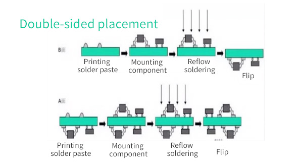
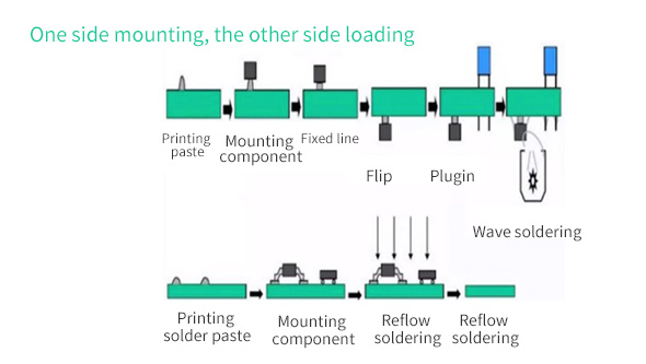
1.Double-sided SMT placement
*In order to maintain the aesthetics and functionality of the PCB, some PCB design engineers use a double-sided mounting method. Among them, the A side is arranged with components, and the B side is mounted with chip components. Make full use of PCB space to minimize PCB area.
*A. Incoming Inspection=> Screen Solder Paste Printing on PCB A side (Dispense surface mount adhesives => Surface Mounting => Drying(Solidifying) => Reflow Soldering on A side => Clean out => Plate Turnover => Screen Solder Paste Printing on PCB B side(Dispense surface mount adhesives) => Surface Mounting => Drying => Reflow Soldering(Better on B side) => Clean out => VI&AOI => Rework/Repair.
This process is suitable for mounting large SMDs on both sides of the PCB such as PLCC.
B. Incoming Inspection=> Screen Solder Paste Printing on PCB A side(Dispense surface mount adhesives => Surface Mounting => Drying(Solidifying) => Reflow Soldering on A side => Clean out => Plate Turnover => Screen Solder Paste Printing on PCB B side(Dispense surface mount adhesives) => Surface Mounting => Solidifying => Wave Soldering on B side => Clean out => VI&AOI => Rework/Repair.
This process is suitable for reflow on the A side of the PCB.
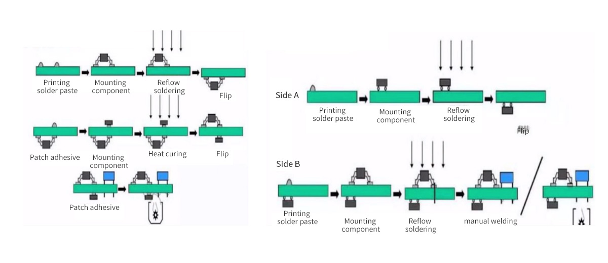
2.Double-sided mixing
The two methods are mixed in the following two ways. The first method is to assemble the PCBA three times for heating, the efficiency is low, and the pass rate of the wave soldering using the red glue process is low. The second method is suitable for the case where there are many double-sided SMD components and there are few THT components, and manual soldering is recommended. Wave soldering is recommended if there are many THT components.
The biggest benefit of designing a double-sided board would be to minimize the footprint. If your project has a strict space requirement, it may be beneficial to move some of the components onto that second size to reduce the space it takes in its end product. The second advantage is that due to the additional layer of copper, there’s increased heat dissipation. During the etching process of fabrication, copper is removed to create tracks but instead of leaving it out completely it is then reinserted.
Products Category
- PCB Design & Layout
- PCB manufacturing
- PCB Assembly
- BGA Assembly
- THT Assembly
- SMT Assembly
- Mixed PCB Assembly in Electronic PCBA
- Single sided PCB assembly
- Double sided PCB assembly
- Rigid-Flex Assembly
- COB Bonding Manufacturing
- Components sourcing for PCB Assembly
- SMT Stencils
- Box build assembly
- PCB engineer reverse
Contact Us
E-mail: [email protected]
E-mail: [email protected]
Skype: [email protected]
Whatsapp: +86 15012972502
Add: 2F, BUILDING H, WANDA INDUSTRIAL ZONE, ZHOUSHI ROAD, LANGXIN COMMUNITY,SHIYAN STREET, BAO 'AN DISTRICT, SHENZHEN, GUANGDONG, CHINA


 Skype Chat
 WhatsApp
  Mail inquiry