

Products >> SMT Stencils
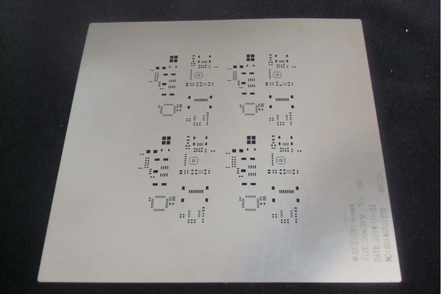
SMT Stencil is one form-stable templates to print solder paste onto the component pads of printed circuit board before the assembly, using a stencil will allow you to apply an even and accurately placed coat of solder paste to the pads. This is often quicker and easier than doing it manually with a syringe, especially if you working with more than one copy of the same board. A consistent and accurate coat of paste will reduce the number of solder bridges and decrease board clean up time.
The list below are the types of stencil.
--Laser cut SMT stencil
--SMT mini stencil
--Led stencil
--Frame SMT stencil
--Frameless stencil
--PCB stencil
--SMT glue Stencil
--Solder paste stencil
--BGA Stencil
How should I choose the stencil size?
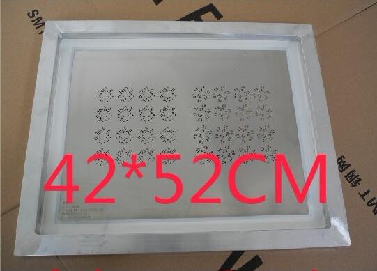
Before customized the stencil,Need to know the assembly machine is Semi-automatic or fully automatic type for the tin scraping.If it’s fully automatic type,suggest to do the size larger than 42cm*52cm.And then check the PCB size to choose the most cost-effective one.
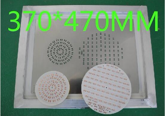
1. Standard stencil size with frame(cm)
*30cmX40cm
*37cmX47cm
*42cmX52cm
*45cmX55cm
*55cmX65cm
*58.4cmX58.4cm
*73.6cmX73.6cm
*40cmX60cm
*40cmX80cm
*40cmX100cm
*40cmX120cm
*40cmX140cm
*50cmX150cm
*50cmX170cm
2. PCB stencil size without frame(cm)
*10cmX10cm
*15cmX15cm
*20cmX20cm
*22cmX22cm
*25cmX25cm
What should be provided for the stencil manufacturing?
Any one of the below listed panelization file is ok for the stencil manufacturing.
--Gerber file
--PCB file
--CAD File
--GBR document
--CAM
--DXF
--PCB bare board
Stencil thickness calculations
The industry standard IPC7525 provides two major parameters for determining the stencil thickness and aperture size:
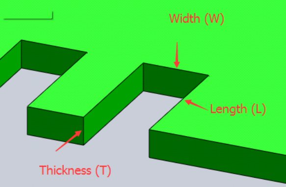
• Aspect Ratio
The width of aperture / thickness = W/T
The lowest acceptable aspect ratio is 1.5.
• Area Ratio
Surface area of aperture / surface area of the aperture walls = L x W/ (2 x (L+W) x T)
The lowest acceptable area ratio is 0.66.
However, there are are special considerations for real PCB assembly. Here are the stencil thickness design principles:
1) The stencil thickness should satisfy the most fine-pitch QFPs and BGAs, while taking into account the smallest chip size.
2) When the QFP pitch ? 0.5mm, the sheet thickness can be selected as either 0.13mm or 0.12mm;
If the pitch> 0.5mm, then the steel thickness can be between 0.15mm - 0.20mm;
If the BGA ball pitch > 1.0mm, then select a 0.15mm thickness.
If the 0.5mm?BGA ball pitch ?1.0mm, then select a 0.13mm thickness.
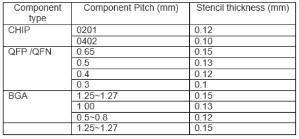
3) It is a priority to select the thickness by BGA or the smallest component if two or more different ICs are simultaneously placed on the board.
4) Step stencil may be applied if the thickness will be 0.1mm for matching a fine pitch component with an area ratio of 0.66, while requiring a 0.13-0.15mm thickness for other components. (Step-down) thickness should be 0.2mm for ceramic BGAs while requiring 0.15mm for other components (Step-up).
If there is any support in need,Please kindly contact us at [email protected]
Products Category
- PCB Design & Layout
- PCB manufacturing
- PCB Assembly
- BGA Assembly
- THT Assembly
- SMT Assembly
- Mixed PCB Assembly in Electronic PCBA
- Single sided PCB assembly
- Double sided PCB assembly
- Rigid-Flex Assembly
- COB Bonding Manufacturing
- Components sourcing for PCB Assembly
- SMT Stencils
- Box build assembly
- PCB engineer reverse
Contact Us
E-mail: [email protected]
E-mail: [email protected]
Skype: [email protected]
Whatsapp: +86 15012972502
Add: 2F, BUILDING H, WANDA INDUSTRIAL ZONE, ZHOUSHI ROAD, LANGXIN COMMUNITY,SHIYAN STREET, BAO 'AN DISTRICT, SHENZHEN, GUANGDONG, CHINA


 Skype Chat
 WhatsApp
  Mail inquiry