

Products >> BGA Assembly
BGA Assembly, The full name of BGA is Ball Grid Array, it is to make an array soldering ball at the bottom of the package substrate as the I/O end of the circuit and interconnect with a printed circuit board (PCB), The device packaged with this technology is a surface mount device.
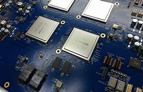
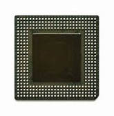
BGA (Ball Grid Array) assembly require special mounting practice experiences. A BGA is an SMD with an array, of solder pads across its bottom side. Instead of using ‘leads’ like normal components use to connect to the PCB, BGA use balls of higher-temperature solder to attach to these pads.It’s used for integrated circuits.Ball Grid Array packages are used to permanently mount devices such as microprocessors.A BGA can provide more interconnection pins than can be put on a dual in-line or flat package.
The whole bottom surface of the device can be used, instead of just the perimeter. The leads are also on average shorter than with a perimeter-only type, leading to better performance at high speeds.
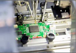
Soldering of BGA devices requires precise control and is usually done by automated processes. BGA devices are not suitable for socket mounting.
Ball grid array packaging is a method for reducing package size and integrating a greater number of functions on a single chip module. BGA (Ball Grid Array) also replaces solder balls on the component underside for SMT mounting.
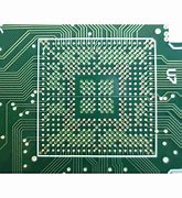
Testing for vias for BGAs and other packages where pads can not be seen from the surface
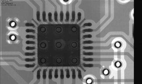
For the components packages including #BGAs and #QFNs,flim chips and CSPs are widely used,Which made solder joints hidden under the packages.This facts makes it impossible for the Manual Visual Inspection,In addition,since the appearance of SMT technology that makes both packages and leads become smaller,traditional inspection methods including optical,ultrasonic and thermal imaging are insufficient. because PCBs have higher density with their solder joints hidden and holes buried or blind.while considering X-Ray inspection system,the trend of both present and future component miniaturization can’t be neglected.Compared with other inspection methods,X-ray is capable of penetrating into inner packaging and inspecting the quality of solder joints.
Assembly of BGAs
Solder dispense
There are a number of deposition techniques that could be used to attach the BGA to the substrate, that include syringe deposition or printing:
1.Syringe deposition
Localised deposition of solder paste in the form of dots, circles or lines can be achieved by depositing controlled amounts through a syringe. The syringe is attached to a head that has x and y axis movement and may also have a height sense feature. The correct amount of material can be dispensed by applying a positive air pressure onto the plunger for a known time through a known needle bore. The viscosity and thixotropy of the material must be controlled so that the material flows easily from the syringe, but will not slump after application.
This technique could be used to deposit a series of dots of solder on to the substrate prior to component attach. This process is very slow and would not be suited to high volume production. However, it has the potential for depositing solder paste during rework.
2.Stencil printing
Stencil printing allows solder paste to be deposited on large areas of the substrate in one operation. A stencil consists of a thin metal foil with apertures cut in it. The aperture through which the material passes can be etched, laser cut or electroformed. Material is deposited through apertures in the stencil when the squeegee traverse's the print area in contact with the top surface, dragging ahead of it the material to be printed. Stencil printing of solder paste, into which the BGA is subsequently placed, is applicable to high volume production.
3.Solder jetting
There are alternative solder deposition techniques, such as solder jet printing, that have the potential to be used in area array attach. In a manner similar to laser jet printing of inks, molten solder can be precisely jetted on to a substrate, or component, to form a solder deposit.
4.Flux only attachment
Flux-only reflow is possible where a tin-lead eutectic or close alloy is used (as in plastic BGA components). Either flux can be deposited on the substrate or the BGA can be flux dipped prior to attachment. The flux will remove any surface oxides present and also holds the BGA in place prior to reflow. An inert gas process is usually required for flux-only reflow to be successful.
5.Pre-assembly inspection
There are a number of reasons why a BGA joint may not be formed upon reflow of the solder ball. Common causes of poor solder joints include insufficient solder paste on the PCB or missing/deformed balls on the component. The solder paste deposited on the substrate can be readily inspected after printing, using modern production line printers equipped with measurement systems or by using off-line measurement systems. The heights of the deposits are monitored using laser measurements, while the position and size of the deposits can be optically verified. Missing solder paste deposits can lead to open joints upon reflow as the solder ball on the component will not have been wetted.
BGA component inspection, prior to placement, is recommended - a process that is routinely carried out in SMT assembly. This inspection step must be capable of identifying whether the solder balls are present or missing. It must also be capable of determining if the size and shape of the balls are consistent. A missing ball should be easy to detect but inspection of components for uniformity of ball shape can be difficult. This is due to the high reflectivity of the solder surface.
Products Category
- PCB Design & Layout
- PCB manufacturing
- PCB Assembly
- BGA Assembly
- THT Assembly
- SMT Assembly
- Mixed PCB Assembly in Electronic PCBA
- Single sided PCB assembly
- Double sided PCB assembly
- Rigid-Flex Assembly
- COB Bonding Manufacturing
- Components sourcing for PCB Assembly
- SMT Stencils
- Box build assembly
- PCB engineer reverse
Contact Us
E-mail: [email protected]
E-mail: [email protected]
Skype: [email protected]
Whatsapp: +86 15012972502
Add: 2F, BUILDING H, WANDA INDUSTRIAL ZONE, ZHOUSHI ROAD, LANGXIN COMMUNITY,SHIYAN STREET, BAO 'AN DISTRICT, SHENZHEN, GUANGDONG, CHINA


 Skype Chat
 WhatsApp
  Mail inquiry