

How to control PCB impedance in design?
How to control PCB impedance in design?
In order to distinguish the resistance of direct current (DC), the resistance encountered by alternating current is called impedance (Z0), including resistance (R), inductive reactance (XC) and capacitive reactance (XL).
PCB characteristic impedance is also called "characteristic impedance". It refers to the resistance of PCB high frequency signal or electromagnetic wave in the transmission signal line (i.e. the copper wire of PCB made by us) at a certain frequency relative to a certain reference layer (i.e. shielding layer, projection layer or reference layer), which is called characteristic impedance in the process of propagation. It is actually the sum of a vector of resistance, inductance, capacitance, etc.
Calculation of impedance PCB:
1. Use the experience value to record the impedance line that has been done before, for example, the line width of PCB and the thickness of the board, and apply it directly in the next use.
2. Firstly, according to the conventional design, highlight the lines that need to be impedance in PCB, and then give the screenshot to the PCB Factory. If the PCB Factory wants to control it, the PCB Factory will modify the data according to the PCB impedance we require, such as adjusting the PCB line width and line spacing to achieve the required impedance.
3. At the beginning of the design: according to the lamination parameters of PCB and the relevant data (PCB board, dielectric constant, green oil, PP thickness, etc.) provided by the PCB manufacturer, we calculated the impedance with si9000 software, and then used the calculated parameters to trace the impedance line, and finally obtained the PCB data to At the same time, the PCB factory needs to control the impedance of PCB. The advantage of this is that in general, the PCB Factory will not move our data, and it is also a very small adjustment.
As you can see from the above,Points 1 and 2 are not safe. In point 1, if the stack parameters of PCB are changed, then the impedance of PCB will also change. I don't know if there is a mistake on the day of continuous application,Point 2. It's OK to click the screenshots to be controlled by the PCB Factory. However, engineers from the PCB Factory often call to say that your PCB impedance can't be done. The reason is that the difference between the line width and line distance of the PCB designed by you is too big, and there is not enough space on the PCB to widen the line width and line distance.Obviously, the third scheme is the safest, and the PCB Factory will not be able to control the impedance of PCB.
Introduction about the Significance of controlling PCB characteristic impedance
PCB not only plays the role of current conduction in electronic products, but also plays the role of signal transmission;
High frequency and high-speed PCB of electronic products require that the circuit performance provided by PCB must ensure that the signal does not reflect in the transmission process and keep the signal intact and undistorted;PCB characteristic impedance is the core to solve the problem of signal integrity.
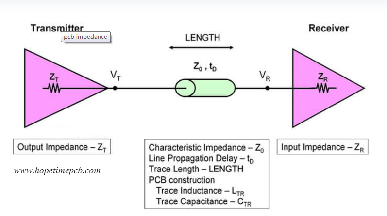
When electronic equipment (such as computer, communication switch, etc.) is operated, the signal sent by driver must reach the receiver through PCB signal line. In order to ensure signal integrity, the characteristic impedance (Z0) of PCB signal line must match the "electronic impedance" of head and tail components;When the transmission line is more than 1 / 3 rise time, the signal will reflect, so PCB characteristic impedance must be considered.
Factors affecting PCB characteristic impedance:
Dielectric constant of PCB is inversely proportional to PCB characteristic impedance (ER)
The dielectric thickness between PCB circuit layer and ground plane (or outer layer) is directly proportional to the characteristic impedance value (H)
PCB impedance line bottom width (lower W1); line surface (upper W2) width, inversely proportional to the characteristic impedance
PCB copper thickness is inversely proportional to PCB characteristic impedance (T)
The distance between adjacent lines of PCB is directly proportional to the characteristic impedance value (differential impedance) (s)
The thickness of PCB substrate solder mask is inversely proportional to the impedance value (c)
Process factors affecting PCB impedance:
Because of etching, when the thickness of copper is more than 2oz, the impedance of PCB can not be controlled.
In the design, there is no copper and wire layer blank, which needs to be filled with curing sheet during production. When calculating the impedance, the thickness of the medium provided by the plate supplier can not be directly replaced, but the thickness of the blank space filled by the curing sheet needs to be subtracted. This is one of the main reasons for the inconsistency between the impedance calculated by ourselves and the results of the manufacturer.
Go to the PCB knowledge Page
Go to the PCB design resources page
Back to the technology data
PCB Blog
Contact Us
E-mail: [email protected]
E-mail: [email protected]
Skype: [email protected]
Whatsapp: +86 15012972502
Add: 2F, BUILDING H, WANDA INDUSTRIAL ZONE, ZHOUSHI ROAD, LANGXIN COMMUNITY,SHIYAN STREET, BAO 'AN DISTRICT, SHENZHEN, GUANGDONG, CHINA


 Skype Chat
 WhatsApp
  Mail inquiry