

PCB Final surface finish comparison
PCB Final surface finish comparison
There are many factors to consider when selecting a final finish for your printed circuit board. Below is a consolidated list of popular finishes and their general characteristics.
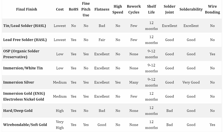
1.Tin/Lead Solder (HASL)
--The PCB is dipped into a solder pot and air knives remove the excess solder from the surface of the board. The typical chemical composition of this finish is approximately 63% Tin and 37% Lead. Historically this has been the accepted industry standard finish but tighter designs and lead free legislation may soon bring this finish to an end for most purposes. Only military, medical and select few other devices that require high dependability are currently exempt from RoHS legislation.
--Pros
Lowest cost and remains solderable through many cycles. Relatively low temperature reflow point.
--Cons
Not recommended for lead pitches less than 0.64mm (.025 inch) due to solder bridging and uneven thickness. Lead is a known cause of many illnesses, more stringent environmental (RoHS lead free) legislature may eventually eliminate this plating option.
2.Lead Free Solder (HASL)
The PCB is dipped into a solder pot and air knives remove the excess solder from the surface of the board. Various chemistries exist for Lead Free Solder but most rely on a 99% Tin composition with various trace elements depending on the manufacturers recipe. While it is flatter than its lead counterpart, Lead Free Solder is still not recommended for fine pitch applications.
--Pros
Lowest cost and remains solderable through many cycles.
--Cons
Not recommended for lead pitches less than 0.64mm (.025 inch) due to solder bridging and uneven thickness. Tin Whiskering is also a concern with tightly spaced features.
3.OSP (Organic Solder Preservative)
A very thin finish. Its only purpose is to protect the bare copper from oxidation since it dissipates after soldering. Assemblers need to use a different type of flux and cannot use as many heating cycles as with other finishes.
--Pros
Low cost, flat surface, good solderability and can be wire bonded.
--Cons
Significant changes to assembly process make it unpopular with most assemblers. Special handling required since finger prints can easily erode the OSP finish exposing the copper to oxidation.
4.Immersion / White Tin
Due to the many other superior alternatives available today, this finish is seldom used.
--Pros
Good solderability, flat surface, low cost.
--Cons
Subject to Tin Whiskering and limited rework capability. Solutions used in manufacturing are suspected carcinogens and pose potential health threats.
5.Immersion Silver
Unlike gold finishes which use a layer of nickel to prevent the base copper from migrating into the metal, silver does not require this process. Silver is applied directly onto the bare copper. Silver is quickly gaining in popularity as a preferred RoHS finish. ENIG is still #1 but time will tell.
--Pros
Good solderability, assemblers like it since it can be worked like HASL. During the solder process the silver is dissolved into the joint providing very good connections, ideal for BGAs.
--Cons
Higher cost than solder but less expensive than ENIG. Tarnishes relatively easily so keep them in a cool, dark place in their original packaging until ready to assemble.
6.Immersion Gold (ENIG) Electroless Nickel Gold
ENIG stands for Electroless Nickel Immersion Gold. Approximately 100-150µ" of nickel is applied directly to the bare copper on the PCB. 2-5µ" of gold are then applied on top of the nickel via a chemical process. Because the gold bonds to the nickel by replacing the outer nickel molecules, the resulting finish is extremely flat and cannot be plated any thicker than approximately 5-6µ".
--Pros
Excellent solderability, flat surface, long shelf life, multiple reflows, will not tarnish easily, precious metal electrical contact surface, mini nickel rivet which strengthens hole walls, and the nickel barrier also protects the barrels from copper dissolution during wave solder and rework.
--Cons
Higher cost, nickel layer is fairly brittle and has been noted to break during mechanical stress. This is known as "black pad" or "mudflat cracks".
7.Hard / Deep Gold
Like all gold finishes, 100-200µ" of nickel is used as a barrier to prevent the copper from migrating into the gold. Because this finish is plated using electricity rather than chemically, the surface is relatively rough. There are hardeners added to the chemistry making the finish very durable. It is generally used for edge fingers or keypad based applications where high durability is desired. Typical gold thickness for this finish range between 7 to 50µ".
--Pros
Durability and long shelf life.
--Cons
High cost, no rework capability and poor coplanarity (flatness).
8.Wirebondable / Soft Gold
Like Hard/Deep Gold, this process is electroplated except this is 99.99% pure gold. Due to its very high cost, it is typically used only for wirebonding applications. Typical gold thickness is between 30-100µ" over 150-200µ" of nickel. Cost varies significantly depending on the desired gold thickness.
--Pros
Long shelf life, solderability and wirebondable.
--Cons
Very high cost and no rework capability.
Click here:Most common used PCB surface finishing comparison
Click here:Advantage and disadvantage for PCB common surface treatment
Click here:Introduction for Surface finish choices
Click here:Tips for PCB Storage with different surface finishing
PCB Blog
Contact Us
E-mail: [email protected]
E-mail: [email protected]
Skype: [email protected]
Whatsapp: +86 15012972502
Add: 2F, BUILDING H, WANDA INDUSTRIAL ZONE, ZHOUSHI ROAD, LANGXIN COMMUNITY,SHIYAN STREET, BAO 'AN DISTRICT, SHENZHEN, GUANGDONG, CHINA


 Skype Chat
 WhatsApp
  Mail inquiry