

The basic knowledge about RF Microwave PCB design
The basic knowledge about RF Microwave PCB design
1.RF and Microwave Layout encompasses the Design of Analog Based Circuits in the range of Hundreds of Megahertz (MHz) to Many Gigahertz (GHz).
2.RF actually in the 500 MHz - 2 GHz Band.(Design Above 100 MHz considered RF.)
3.Microwave above 2 GHZ.
4.Unlike Digital, Analog Signals can be at any Voltage and Current Level (Between their Min & Max), at any point in Time.
5.Standard Analog Signals are assumed to be between DC and a few Hundred MHz.
6.RF/Microwave Signals are One Frequency or a Band of Frequencies imposed on a Very High Frequency Carrier.
7.RF/Microwave Circuits are Designed to Pass Signals within Band of Interest and Filter Energy outside that Range.
8.Signal Band can be Narrow or Wide.
*Narrow Band Circuits usually have Pass Band less than 1 MHz.
*Broad Band Circuits Pass a Range of Frequencies up to 10’s of MHz.
9.When Digital and Microwave exist in the Same Unit, Pass Bands of Microwave Circuits usually fall (by design) Outside the Harmonic Range of the Digital Signals.
10.RF / Microwave PC Board Layout simply follows the “Laws of Physics”-
11.When Laws of Physics can’t be followed,Know what Compromises are available.
12.Microwave Signals are Very Sensitive to Noise, Ringing and Reflections and Must be treated with Great Care.
13.Need Complete Impedance (Zo) Matching (50 ohm out/ 50 ohm line/ 50 ohm in).
*Minimizes Return Loss / VSWR.
14.A Transmission Line is any Pair or Wires or Conductors used to Move Energy From point A to point B, Usually of Controlled Size and in a Controlled Dielectric to create a Controlled Impedance (Zo).
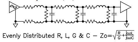
15.Inductance (L) is Determined by the Loop Function of Signal and Return Path.
*Small Spacing (Tight Loop) creates High Flux Cancellation, hence Low Inductance.
16.Capacitance (C) is Function of Signal spacing to the Return Path.
*Small Spacing creates High Capacitance.
17.Since Small Spacing (Tight Loop) creates Low L & High C and since Zo = sqrt L/C,Small Spacing creates Low Zo.
18.Additionally, Zo is function of Signal Conductor Width & Thickness and a Function of the Dielectric Constant ( ) of the Material surrounding the Lines.
19.Sometimes Dielectric surrounding Transmission Line isn’t Constant (Outer Layer Trace on PCB).
*DK above Trace is Air ( = 1.0008).
*DK below Trace is FR4 (approx = 4.1).
*Effective Relative ![]() is 3 to 3.25.
is 3 to 3.25.
20.Equations given later to Calculate Effective Relative ![]()
21.Signal Return Currents follow the Path of Least Impedance (In High Frequency Circuits that = Path of Least Inductance).
22.Whenever we Neglect to provide a Low Impedance Return Path for RF / Microwave signals, they WILL find a Path.
23.It may NOT be what we had in mind.
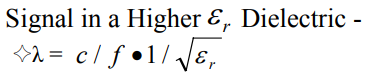
24.Signal Wavelength -
*Wavelength (λ) of a Signal is the Distance it Travels in the Time of One Cycle.
25.For a Signal Traveling in Free Space -
*λ = c (Speed of Light) / f (frequency).
(λ = 11.78”/nSec at 1GHz = 11.78”)
26.
27.Signal Critical Length-
*How long a PCB Trace can be before we MUST pay attention to Impedance Control.
*Function of Frequency (1/16th Wavelength)
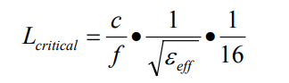
28.At 1 GHz = approx .425” (Microstrip- FR4)
29.At 1 GHz = approx .375” (Stripline - FR4)
30.Signal Loss / Noise -
*Reflections -
--Return Loss / VSWR
*Skin Effect -
--Increased Resistance of PCB Trace due to Decreased Cross Sectional Area.
--In Analog Circuits above 100 MHz.
--Skin Depth- .000822” @ 10 MHz.
.000026” @ 10 GHz.
*Loss Tangent -
--Dielectric Loss caused by Molecular Structure of Board Material.
--In Analog Circuits above 200 MHz.
--PTFE’s Far Better than FR4.
*Energy Coupling-
--Cross Talk.
--Noise Induction.
To know more:
Guidelines for RF & microwave PCB Design
The basic knowledge about RF Microwave PCB design
Recommend reading list for RF/Microwave PCB design
PCB Blog
Contact Us
E-mail: [email protected]
E-mail: [email protected]
Skype: [email protected]
Whatsapp: +86 15012972502
Add: 2F, BUILDING H, WANDA INDUSTRIAL ZONE, ZHOUSHI ROAD, LANGXIN COMMUNITY,SHIYAN STREET, BAO 'AN DISTRICT, SHENZHEN, GUANGDONG, CHINA


 Skype Chat
 WhatsApp
  Mail inquiry