

The Industrial Process of Printed Circuit Board Assembly
The Industrial Process of Printed Circuit Board Assembly
What is PCBA means?
PCBA means Printed Circuit Board Assembly,is the process of connecting or the assembly of components and wirings onto a printed circuit board to give the final result.
Basic requirements for Printed Circuit Board Assembly
1.Printed Circuit Board
2.Electrical components
3.Soldering Materials (depend on the type of soldering) for example, solder wire, solder paste etc.
4.Soldering Flux
5.Equipment for Soldering for example, soldering station, wave soldering machine,testing equipment.
PCB Assembly Process:The assembly could be of two types,PTH and SMT
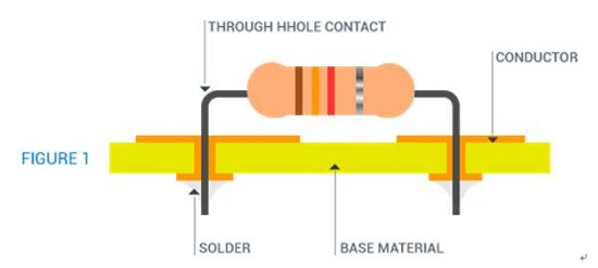
Type 1: PTH (Plated Through-hole Technology):
Through-hole technology is the mounting of electronic components, involving the use of leads that are inserted into holes drilled into the PCB and are then soldered on the opposite sides either manually or by automated mounting machines.
Wave Soldering: Wave soldering is a soldering process which involves the use of waves and molten solder to attach electrical components onto the PCB. Essentially, the board is passed over a pan of molten solder. A pump below produces an upwelling almost like a wave of solder. The solder is at high temperature, its range depending on the type of solder. The PCB is passed over the molten solder bath by the help of a conveyer belt, and the components are soldered onto the board. The whole process has the following steps
1: Insertion of electronic components: The various components are first to be assembled into the board.
2: Fluxing: Fluxing is designed to improve the mechanical strength in solder joints. It can be corrosive or non-corrosive. The primary objective is to clean the components that are to be soldered.
3: Preheating: Preheating helps to accelerate the soldering process.
4: Cleaning: The flux residues along with other residues are cleaned basically by solvents or demonized water.
5: Testing:Testing is done to ensure the PCB is of proper quality and has no defects. Hand Soldering:It is the oldest form of soldering. Hand soldering is done in low bulk quantity. Most common in rework or repair jobs. Hand soldering uses an iron, solder, soldering wick, and flux to attach components to a circuit boards. Sometimes. PCBs that are rejected or are faulty are hand soldered to remove the defects.
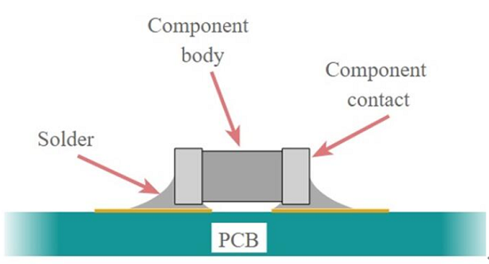
Type 2:SMT (Surface Mount Technology):
This technique is widely in use by many PCB manufacturers. The process involves components with metal tabs that can be easily soldered onto the PBC. SMD (Surface Mount Device) don’t have leads or legs. Therefore the process is different from through-hole soldering process.
1.Materials Preparation: Prepare the PCB boards, components, PCB stencil and solder paste, Gerber file, and necessary tools (soldering iron, wire stripper, torch, heat gun etc.)
2.Bare Board Baking: Ensure the humidity of your PCB is low.
3.Solder Paste Printing: Solder paste is used to connect the surface mount components into the board.
4.Pre-Solder Inspection: Check the PCBs for any problem prior to soldering
5.High Speed Mounting: SMT component placement systems also called pick and place machines are used to place the components accurately to the PCB.
6.Visual Inspection prior to Re-Flow: Checking again prior to re-flow soldering for any problem.
7.Re-Flow Soldering:Next, solder paste is used to attach the components into their contact pads after which the assembly is heated. As a result, the solder melts permanently connecting the joint.
8.AOI:Automated Optical Inspection is the visual inspection of PCB where an AOI instrument is used to scan the device for errors or defects.
9.DIP plug-in processing: Next there is a simple processing of the plug-in material and insertion of the corresponding position of the board.
10.Wave Soldering: Next, the plugged board enters the wave soldering process. The soldering is done though spray welding, fluxing, pre heating and wave peak soldering after which the PCB is cooled down.
11.Cleaning: After soldering, the electronic assemblies are cleaned to remove excess solder flux.
12.ICT/FCT: In-circuit and function test in which all components are measured and tested in order to ensure the proper functioning of the PCB.
13.Quality Checking: The product is sent for quality inspection to make sure the quality fits the demand.
14.Packing:Last, the PCBs are packed and then are shipped off to the customers.
PCB Blog
Contact Us
E-mail: [email protected]
E-mail: [email protected]
Skype: [email protected]
Whatsapp: +86 15012972502
Add: 2F, BUILDING H, WANDA INDUSTRIAL ZONE, ZHOUSHI ROAD, LANGXIN COMMUNITY,SHIYAN STREET, BAO 'AN DISTRICT, SHENZHEN, GUANGDONG, CHINA


 Skype Chat
 WhatsApp
  Mail inquiry