

What is a via hole in PCB?
What is a via hole in PCB?
A VIA hole in a PCB consists of two pads in corresponding positions on different layers of the board, that are electrically connected by a hole through the board. The hole is made conductive by electroplating.
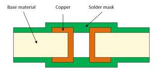
Via Hole
A via consists of:
*Barrel — conductive tube filling the drilled hole
*Pad — connects each end of the barrel to the component, plane or trace
*Antipad — clearance hole between barrel and no-connect metal layer
A via may be at the edge of the board so that it is cut in half. This is known as Plated Holes on the Board edge and is used for a variety of reasons, including allowing one PCB to be soldered to another.
Via holes have a tolerance of +0.10/-0.30mm and can therefore be reduced to accommodate a larger annular ring. We have set a threshold value for this at 0.45mm but it can be altered by our customer in the order details. The threshold means that all PTH holes equal or smaller than the given diameter are seen as via holes and thus can be reduced.
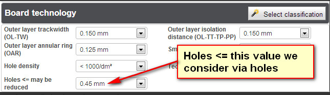
Hole diameter considered as via hole.
Go to the PCB knowledge Page
Go to the PCB design resources page
Back to the technology data
PCB Blog
Contact Us
E-mail: [email protected]
E-mail: [email protected]
Skype: [email protected]
Whatsapp: +86 15012972502
Add: 2F, BUILDING H, WANDA INDUSTRIAL ZONE, ZHOUSHI ROAD, LANGXIN COMMUNITY,SHIYAN STREET, BAO 'AN DISTRICT, SHENZHEN, GUANGDONG, CHINA


 Skype Chat
 WhatsApp
  Mail inquiry