

What is the TOP side of a PCB?
What is the TOP side of a PCB?
In your PCB layout you define a side/layer TOP side of the PCB. Hence layers present on that side of your PCB will be called TOP xxx. Examples are TOP circuit layer, TOP solder mask, etc…
The TOP side of the PCB is usually the side where the components are placed and therefore sometimes also called COMPONENT side. However more often, PCB are populated on both sides and thus is the naming TOP more clear as definition.
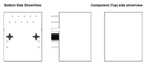
What is the difference between the component (top) side show/view and the bottom side view?
The component side show or the component side view is a top side view (view thought the component).The bottom side view is the view from the bottom side of the component. Basically bottom side view is mirrored top side view.
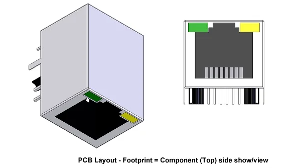
What view should you use while drawing the footprint (land pattern) for the PCB layout of the electronic’s parts?
When you draw the PCB layout (footprint), you should draw the component side view. For details, see picture 1.
PCB Blog
Contact Us
E-mail: [email protected]
E-mail: [email protected]
Skype: [email protected]
Whatsapp: +86 15012972502
Add: 2F, BUILDING H, WANDA INDUSTRIAL ZONE, ZHOUSHI ROAD, LANGXIN COMMUNITY,SHIYAN STREET, BAO 'AN DISTRICT, SHENZHEN, GUANGDONG, CHINA


 Skype Chat
 WhatsApp
  Mail inquiry