

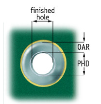
What is the Diameter of PHD and Tooling holes on PCBs?
What is the Diameter of PHD AND Tooling holes on PCBs?
Tooling holes on PCBs are added for a variety of reasons depending on the requirements of the equipment being used. They are mainly used to aid in PCB alignment and orientation for drilling and routing during assembly . We at Hopetimepcb apply tooling holes to panelized boards when specified , and our hole size must be in the range of 0.8mm to 4.0mm. For typical tooling holes, Hopetimepcb suggests to drill tooling holes at the standard size of 2.0mm.
A hole diameter or PHD refers to a production tool’s diameter that you use to drill holes.So, the calculation of a hole size diameter differed for non-plated through holes and plated through holes.
The production hole diameter (PHD) is the diameter of the tool used in production to drill the hole.
Production Hole Diameter or Toolsize = Finished Hole Size plus:
1.+ 0.10mm/4mil for Plated Through Holes
2.+ 0.00mm/0mil for Non Plated Through Holes
3.PHD – finished hole size = copper plating finish + applied finish
The difference in diameter between PHD and the finished hole size for plated through holes is the copper plating in the hole and the applied finish (HAL, ENIG, etc…)
Hole Diameter--OAR (Outer layer Annular Ring)
The OAR is the outer layer annular ring. And you can calculate it by dividing the difference between the copper pad diameter and tool size by 2.

FAR (Finished Annular Ring)
The Finished Annular Ring is the part that lies between the solder hole and the external solder pad rim.Plus, the annular ring breaks when the drilled hole is off the center.But it's all dependent on the external diameter of the solder pad against the nominal hole size diameter.
Calculation of FAR;
The width (T1) of the finished annular ring on external layers should be >= 0.050 mm for the board.
The width (t2) of the annular ring on inner layers should be >= 0.0100 mm for the board.
Go to the PCB knowledge Page
Go to the PCB design resources page
Back to the technology data
PCB Blog
Contact Us
E-mail: [email protected]
E-mail: [email protected]
Skype: [email protected]
Whatsapp: +86 15012972502
Add: 2F, BUILDING H, WANDA INDUSTRIAL ZONE, ZHOUSHI ROAD, LANGXIN COMMUNITY,SHIYAN STREET, BAO 'AN DISTRICT, SHENZHEN, GUANGDONG, CHINA


 Skype Chat
 WhatsApp
  Mail inquiry