

Peel-off Mask
PCB Design Guidelines-Peel-off Mask
A peelable soldermask is screen printed and used in order to protect selected solder holes against plugging during mass soldering. A peelable soldermask can also protect carbon elements and gold plated contacts during mass soldering.
Generating Output
Please ensure that you include the board outline in your peel-off layer(s).
This is best drawn using a small line – e.g. 0.500mm (20mil) wide where the center of the line is the exact board outline.We will remove this line from the production data we use to manufacture your boards.
Peel-off Mask Design Rule Specifications
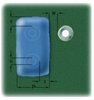
*Minimum width of any Peel-off element (P): 0.500mm (20mil)
*Maximum coverable hole ENDSIZE (H): 6.00mm (236mil)
*Minimum overlap on copper pattern (V): 0.600mm (24mil)
*Minimum clearance to free copper (W): 0.600mm (24mil)
*Minimum distance from PCB outline: 0.500mm (20mil)
*Tolerance on position: +/-0.300mm (12mil)
Avoid using many different small peel-off areas randomly placed on your PCB.We recommend making the peel-off areas as large as possible, this will make them easier to remove after the soldering process.To achieve this connect separate peel-off areas together wherever practical.
Peel-off masks are used to:
*Protect selected solder holes and pads against solder plugging during mass soldering.
*Protect gold-plated contacts or carbon elements during mass soldering.
Application
Usually, the peel-off mask is only applied to 1 side of the PCB, usually the bottom side.
IMPORTANT
If you require Peel-off mask on the top or bottom side of the PCB please ensure this is clearly indicated.This should be done by using correct file naming and clear buildup or layer sequence description in the Mechanical layer.See PCB Design Guidelines – Input Data Requirements and Mechanical Layer pages.
Go to the PCB knowledge Page
Go to the PCB design resources page
Back to the technology data
PCB Blog
Contact Us
E-mail: [email protected]
E-mail: [email protected]
Skype: [email protected]
Whatsapp: +86 15012972502
Add: 2F, BUILDING H, WANDA INDUSTRIAL ZONE, ZHOUSHI ROAD, LANGXIN COMMUNITY,SHIYAN STREET, BAO 'AN DISTRICT, SHENZHEN, GUANGDONG, CHINA


 Skype Chat
 WhatsApp
  Mail inquiry