

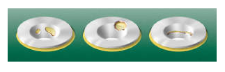
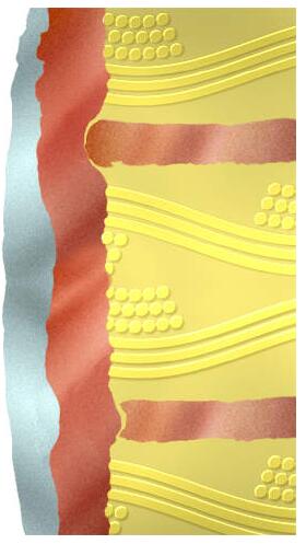
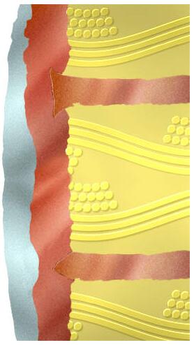
The micro section of a PTH in PCB
The micro section of a PTH in PCB
To check the quality of PTH after the galvanic process we measure the Cu plating thickness of several holes on every production panel.
On every production panel we include test coupons. From every production batch we select some coupons and make micro sections of the PTH to check the quality of the PTH in the final PCB.
Effects that we may spot but as Eurocircuits want to avoid in production are:
Voids
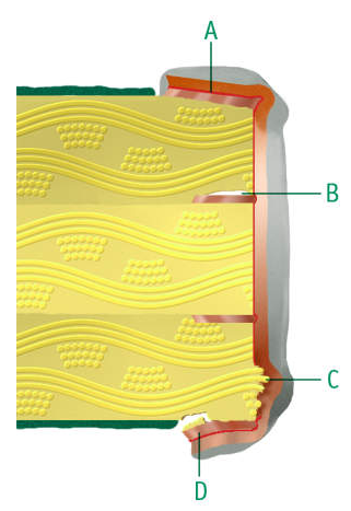
1.Not more than 1 void per test coupon or individual PCB.
2.Plating void in excess of 5% of the PCB thickness.
3.Voids at the interface of an inner layer.
4.Circumferential void in excess of 90° (circumferential crack).
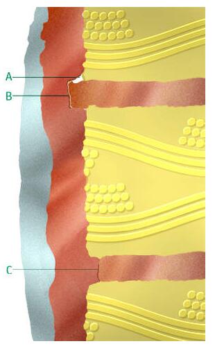
Acceptable on the condition that :
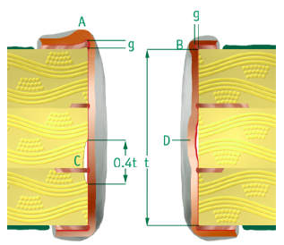
1.The hole wall exhibits an otherwise smooth and coherent structure. (A)
2.No sign of cracks around the nodule-area. (B)
3.The minimum Cu-thickness is fulfilled.
4.Do not reduce the hole diameter below the absolute minimum requirements.
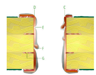
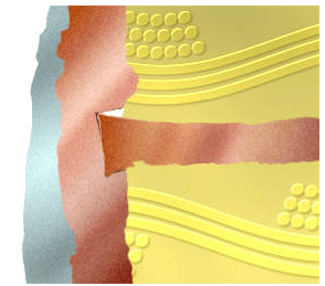
Cracks are not acceptable before or after thermal stress, accept for Foil cracks (D)(C) after thermal stress not extending the through plating.
Other typical cracks:
(E) Barrel crack – not permitted before or after terminal stress.
(F) Crack around nodule – not permitted before or after terminal stress.
(G) Crack in inner pad or inner Cu-layer – not permitted before or after terminal stress.
(H) Foil-crack – is permitted after thermal stress only on outer layers, provided it does not extend through plating.
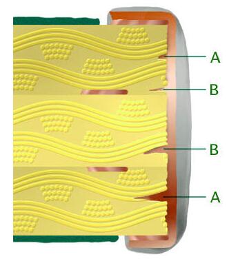
Roughness
Permitted if not reducing plating thickness below min
Burrs
Burrs (A, B) are acceptable if they do not reduce the hole diameter below the required minimum.
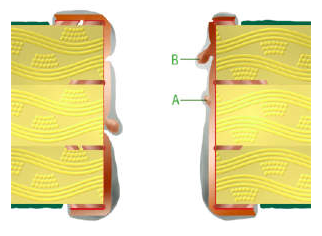
Plating separation
Plating separation between laminate and hole wall is acceptable if extending over no more than 40 % of the PCB-thickness (t). The separation can occur as :
resin recession around the hole wall (C)
hole wall pull-away (D)
Inter plane separation
Not permitted.
Pad rotation (A)
Permitted.
Pink ring (B)
Permitted.
Glass fiber protrusion (C)
Permitted if not reducing hole diameter or Cu-thickness below minimum.
Lifted land (D)
Only allowed after thermal stress or rework simulation
Wicking
Permitted if not exceeding 100 micron (A).
And not reducing min. conductor spacing (B).
Epoxy
smear Epoxy smear or other form of separation (d-effect) is not allowed between plated hole wall and inner pads
Nail heading
Permitted providing there is no evidence of separation
Arrow Heading
Permitted providing there is no evidence of seperation
Shadowing(A)
Permitted
Positive etch back (B)
Etch back of smear and dielectric material : max. 80 micron.
Negative etch back (C)
Smear removal and etch back of internal Cu-foil : max. 25 micron.
Burned plating
No heavy burned surfaces permitted
Go to the PCB knowledge Page
Go to the PCB design resources page
Back to the technology data
PCB Blog
Contact Us
E-mail: [email protected]
E-mail: [email protected]
Skype: [email protected]
Whatsapp: +86 15012972502
Add: 2F, BUILDING H, WANDA INDUSTRIAL ZONE, ZHOUSHI ROAD, LANGXIN COMMUNITY,SHIYAN STREET, BAO 'AN DISTRICT, SHENZHEN, GUANGDONG, CHINA


 Skype Chat
 WhatsApp
  Mail inquiry