

Options and Requirements for Solder Mask
Options and Requirements for Solder Mask
1.Introduction
The solder mask is a piece of the Printed Circuit Board (PCB) fabrication process that is often taken for granted, but this piece is absolutely vital in assuring the quality and functionality of a PCB. The striking difference in quality between boards with and without solder masks is the reason why we at Hopetimepcb include solder masks as a standard finish on all our boards. Having established the importance of solder masks, it follows that a PCB designer should understand the function of a solder mask in some detail and the types offered by their manufacturer.
2.What is a Solder Mask?
A solder mask is a robust, permanent coating that is laminated over the copper traces of a PCB. This layer is sometimes called the“solder stop mask” or “solder resist”. The main function of a solder mask is to prevent the formation of solder bridges during automated mass assembly. A solder bridge is formed when a small bead of solder creates an unintended electrical connection between two or more pads on a PCB. An additional purpose of a solder mask is to protect the copper traces against oxidation, which substantially improves the lifetime of the board.
The solder mask becomes even more essential in the mass assembly of PCBs, where a solder bath is used to tin each copper pad. During this process, the solder mask acts to ensure that no traces of solder are left in unintended areas as a result of the solder bath. Such trace amounts of solder could cause a short circuit between two points on the board, which should be unconnected.
3.Types of Solder Mask
At Hopetimepcb , we offer Liquid Photo -Imageable solder mask , and peel-able solder mask (described in section 7.7). Liquid Photo -Imageable (LPI) solder masks are composed of an ink compound that can be silkscreened or sprayed onto the PCB. The LPI solder mask technique is commonly used with hot air surface levelling (HASL), and requires a clean environment, free of particles and contaminants, for application. After an LPI solder mask is applied, and the PCB is completely covered on both sides with the solder mask, the next stage in the process is curing.
Unlike some older solder masks, LPI inks are sensitive to UV light and can be cured after a short “tack cure cycle”, making use of UV light exposure. This curing process cements the solder mask in place permanently. To ensure that the LPI mask is cured in the proper locations, negative film stencils of the top and bottom solder masks are printed using a contact printer and the original Gerber files. The film sheets are printed with black sections corresponding to any areas of the PCB that are to be left uncoated for soldering, or otherwise free from the solder mask. The entire PCB is then exposed to a UV light, which causes the solder mask to cure and harden in any exposed areas, but has no effect on those areas shielded by the black film. After curing is complete, the uncured mask can be washed off of the film-shielded sections, leaving the solder mask in only the desired areas.
Our high-quality solder mask is durable and long-lasting. Usually, we consider that a 1um solder mask layer can withstand 100 VDC. We can ensure the solder mask thickness will be minimum 5um on the conductor corner and minimum 10um on conductor surface. These thicknesses ensure that for the majority of designs,breakdown of the solder mask is not an issue.
4.Solder Mask Design Rules
When starting a new PCB layout, or before submitting your design to Hopetimepcb for PCB Fabrication,it is worthwhile to check your solder mask spacing against the following criteria to ensure manufacturability:
Conductor Overlap: Refers to the relative size of the solder mask, compared to the copper feature.Hopetimepcb requires a conductor overlap at least 4 mil larger than the feature size.
Solder Mask Clearance: Related to conductor overlap, the solder mask clearance defines the actual space between the edge of the copper feature and the edge of the solder mask. Hopetimepcb requires a minimum solder mask clearance of 2 mil.
Solder Mask Bridge: Refers to the width of the solder masked area that fills a gap between any two pads on the PCB. Hopetimepcb prefers a minimum solder mask bridge of 4 mil, with an absolute minimum of 3.5 mil.
Figure 1 below shows a visual depiction of the spacing requirements described above for clarity.
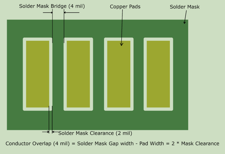
Figure 1:Visual Depiction of Solder Mask Spacing Requirements
5.Solder Mask Colours
The colour of a solder mask has no effect on the electrical performance of a board, but there is an important aspect of contrast between traces, planes, and empty space to consider. Solder masks are available in a variety of colours, including some standard colours and a large variety of custom colours. The colour chosen can make quite a difference in the degree of difficulty for future troubleshooting of the PCB. We at Hopetimepcb have a number of standard solder mask colours available, but custom colours will need to be ordered in advance.
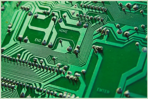
Figure 2: A Standard Green Solder Mask Protecting Copper Traces
--Standard Solder Mask Colours
We at Hopetimepcb offer the following standard solder mask colours: Green, Matte Green, Red, Blue, Matte Blue, Yellow, Black, Matte Black, and White.
Green
In terms of practical performance, green is the best choice for the solder mask colour. It is the industry standard because green is easy on the eyes, allowing for high contrast between traces, planes, and empty space on the PCB. High contrast allows for technicians to easily check, with the naked eye, for manufacturing defects.
Red
Red is a colour that looks professional, but the contrast between traces, planes, and empty space is lower than it is with a green solder mask. Some degree of magnification is suggested when inspecting fine traces on the board for defects with this colour.
Blue
Blue solder masks show a low contrast between traces, planes, and empty space; thus, magnification is mandatory when inspecting for manufacturing defects. These PCBs look aesthetically pleasing and very professional, making them a good choice for fully-developed finished products that will not require much trace visibility.
Yellow
Yellow solder masks show very high contrast between planes, traces, and empty spaces. In fact, the contract achieved by the use of a yellow mask is as high as green; however, the colour is unpopular.
Black
Black is a glossy colour that looks good but has almost no contrast between traces, planes and empty space. Black also absorbs heat, which increases the danger of overheating for sensitive components.
White
White has the lowest contrast and is also the hardest to clean. If possible, we avoid choosing white.
--Custom colour
We at Hopetimepcb are happy to offer custom solder mask colours, such as purple and orange, but we do not keep these colours in stock. We will need to purchase these colours prior to production, so we employ a Minimum Order Quantity (MOQ) for custom colours. Expect a marginal increase in both price and turn time for your PCBs if you select a custom colour for the solder mask.
6.Substitutes (North America vs China)
Hopetimepcb offers high-quality Taiyo solder mask oil, which has satisfied the requirements of most clients and is available in North America as well. Taiyo is the world 's leading manufacturer of specialty inks and solder masks for printed circuit boards.
7.Solder Mask Tenting
Solder masks can be used for covering the holes in a PCB by a process called tenting, the goal of which is to minimize the amount of exposed conductive material on the surface of the board in the interest of preventing shorts. We recommend tenting only for vias, and not THT pads, because some solder mask oil will flow into the holes during the tenting process, and this might affect the finished hole size.
8.Solder Mask Plugging
We also offer solder mask plugging in which holes are plugged with solder mask oil on both sides. These should be indicated in your Gerber files. Hole sizes for plugging should be smaller than 0.5mm (20mil) in diameter.
9.Peel-Able Solder Mask
A peel-able solder mask (PSM) is a type of temporary solder mask that is selectively applied to parts of a PCB.It is used to protect gold plated surfaces from being coated with solder before the Hot Air Solder Leveling(HASL) process, and then it isremoved manually. If a peel-able solder mask is used to cover holes on a PCB, the mask’s area should be 0.3mm bigger per side than the holes. Also, it should avoid any pads not required to be covered by at least 0.4mm.
Go to the PCB knowledge Page
Go to the PCB design resources page
Back to the technology data
PCB Blog
Contact Us
E-mail: [email protected]
E-mail: [email protected]
Skype: [email protected]
Whatsapp: +86 15012972502
Add: 2F, BUILDING H, WANDA INDUSTRIAL ZONE, ZHOUSHI ROAD, LANGXIN COMMUNITY,SHIYAN STREET, BAO 'AN DISTRICT, SHENZHEN, GUANGDONG, CHINA


 Skype Chat
 WhatsApp
  Mail inquiry