

What is the Buildup of a PCB?
What is the Buildup of a PCB?
A PCB is defined by the designer with a number of copper layers in a define sequence that is known as Buildup or Board Buildup.The pattern in each copper layer combined with the drill patterns and the copper plating of these drilled holes, form an electrical net that is responsible for connecting the pins of components to other pins of other components.This makes it possible that currents can flow and the application can function.
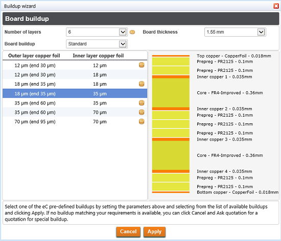
The Buildup or Board BUILDUP of a PCB is the sequence in which these copper layers are defined.
The figure 1 shows a Sample 6-layer board buildup wizard.
Go to the PCB knowledge Page
Go to the PCB design resources page
Back to the technology data
PCB Blog
Contact Us
E-mail: [email protected]
E-mail: [email protected]
Skype: [email protected]
Whatsapp: +86 15012972502
Add: 2F, BUILDING H, WANDA INDUSTRIAL ZONE, ZHOUSHI ROAD, LANGXIN COMMUNITY,SHIYAN STREET, BAO 'AN DISTRICT, SHENZHEN, GUANGDONG, CHINA


 Skype Chat
 WhatsApp
  Mail inquiry