

What is Conductor Clearance in PCB?
What is Conductor Clearance in PCB?
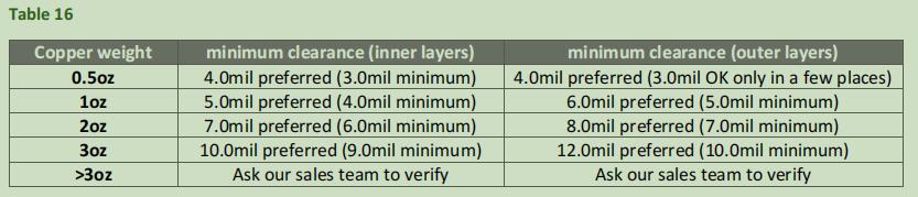
Conductor clearance is the distance between traces or other copper elements. Sufficient trace clearance is essential to ensure manufacturing tolerances do not compromise the function of your board. In addition, to ensure the conductor width can match the Gerber, we must compensate (or enlarge) the conductor in Gerber to counteract the effect of undercut, as explained in Etch Factor. The heavier the copper weight is,the deeper the etching, thus wider conductor clearance is needed to compensate.The minimum conductor clearance depends on the copper weight, as shown in Table 16 below.
Copper traces and other features must also be kept at least 0.2 mm (8 mil) from the board edge for standard tab routing, or 0.4 mm (16 mil) for V-Scoring. Feature-to-edge requirements are intended to protect against potential damage to copper features when individual boards are separated from the fabrication panel.
Go to the PCB knowledge Page
Go to the PCB design resources page
Back to the technology data
PCB Blog
Contact Us
E-mail: [email protected]
E-mail: [email protected]
Skype: [email protected]
Whatsapp: +86 15012972502
Add: 2F, BUILDING H, WANDA INDUSTRIAL ZONE, ZHOUSHI ROAD, LANGXIN COMMUNITY,SHIYAN STREET, BAO 'AN DISTRICT, SHENZHEN, GUANGDONG, CHINA


 Skype Chat
 WhatsApp
  Mail inquiry