

What is Micro-via?
What is Micro-via?
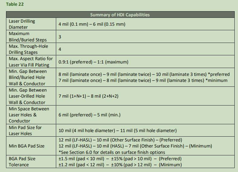
A standard micro-via consists of tiny copper-plated holes with a diameter of 6mil (0.15mm) or less and are made using a laser drill. Micro-vias can connect adjacent layers, allowing a single multilayer PCB to hold more circuit traces, which increases PCB circuit density. Although a single standard micro-via can only link two adjacent copper layers, there will still be significantly more available space for traces. Micro-vias consisting of various types such as blind via and buried via are used in High-Density Interconnect (HDI) PCB designs. Via-in pad technology is also available, as described in Section 4.9, to further increase circuit density.A standard micro-via is a highly reliable type of interconnection structure and should be used in a board design whenever possible. For an HDI PCB, the circuit routes need to interconnect several layers to connect components, but a standard micro-via can only be used to connect two adjacent layers. Thus, in order to use micro-via in HDI board design, we need to use the micro-vias in a compound design structure to connect more than two adjacent layers. There are two types of complex structures that use a standard micro-via: staggered and stacked structures. These structures are described below in sections 5.3.3 and 5.3.4.
We at Hopetimepcb can fabricate micro-via with a size ranging from 4mil (0.1mm) to a maximum size of 6 mil (0.15mm). Fabrication of these vias will require separate drill filesfor each layer pair, with the via hole positions on all of the different layers of a multi-layer PCB; for example, one drill file for all top-to-bottom layer holes, and another for all second-to-third layer holes, etc.
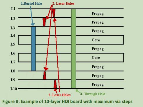
An HDI PCB board layer with buried and blind vias can be laminated on the same side a maximum of three times. This means that a board can be processed in a maximum of 3 stepsfor blind or buried vias. For example,as boards are built from the center, we can have a buried via through a center layer, then a second process can add layers on either side with more buried vias and then a third pressing can add blind vias to the outer layers.Finally, through-holes can be drilled for a total of 4 drilling stages. See Figure 8 below
Go to the PCB knowledge Page
Go to the PCB design resources page
Back to the technology data
PCB Blog
Contact Us
E-mail: [email protected]
E-mail: [email protected]
Skype: [email protected]
Whatsapp: +86 15012972502
Add: 2F, BUILDING H, WANDA INDUSTRIAL ZONE, ZHOUSHI ROAD, LANGXIN COMMUNITY,SHIYAN STREET, BAO 'AN DISTRICT, SHENZHEN, GUANGDONG, CHINA


Link
 Skype Chat
 WhatsApp
  Mail inquiry