

Blind and Buried Vias
Blind and Buried Vias
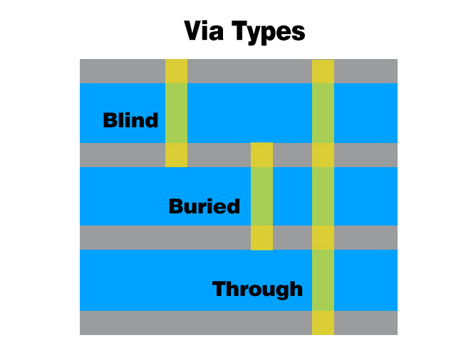 Figure 1
There are 3 kinds of Vias as Figure 1 showed.
1.Blind vias:A blind via connects an outer layer of the board to inner layers and doesn’t go through the entire board.
2.Buried via:A buried via connects inner layers without reaching the outer layers.
3.Through hole:A through hole via goes all the way through, from top to bottom, connecting all layers.
Sometimes, you can’t fit all your connections on one layer. This is where vias come to your rescue!
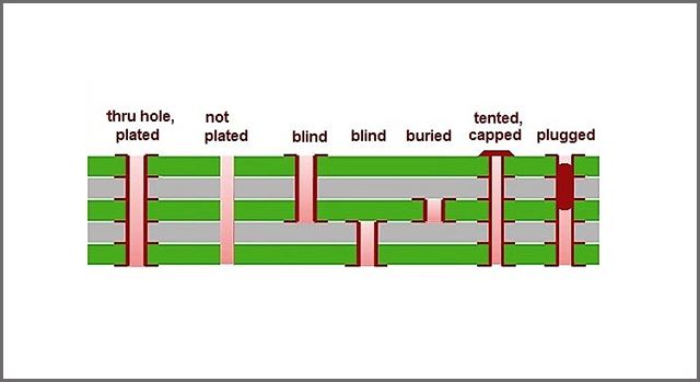
Vias are barrel shaped vertical conductive holes that make connections between multiple layers of a PCB. The IPC defines eight different types of vias, but we’re going to talk about blind and buried vias; the two you’re most likely to work with.
Blind and Buried Vias Within Layout
You can easily configure your vias within the constraint manager in the physical workspace. Standard clearance rules apply when placing the vias. It is not recommended to place a via directly between pads of a surface mount component (SMD) as solder flux could potentially get trapped and cause corrosion problems. If solder flux would be under the SMD, inspecting and diagnosing the issue between a pad and via would be difficult once the board is manufactured and assembled.
How Do manufacturer the vias?
Vias are manufactured in two ways: either after or before multilayer lamination. When blind and buried vias are created, one or more of the cores are drilled and the through holes are plated. Then the stack is built and pressed. You can read more about the manufacturing process in the IPC-2221B manual.
When creating blind vias, it is important to be aware of the drill depth. Depending on how shallow or deep the hole is, it could have a negative impact on the board. If the hole is too deep then it may cause signal distortion or degradation, and if it’s too shallow then it could result in an improper connection.
It's best to consult with your PCB manufacturer to get advice on the best approach to design your board to avoid a costly manufacture. Make sure to have your manufacturer plug the vias with either metal or thermal/electrical epoxy and plate copper over it; or else internal air bubbles can migrate upwards and lead to voids or pin holes in the solder joint.
Go to the PCB knowledge Page
Go to the PCB design resources page
Back to the technology data
PCB Blog
Contact Us
E-mail: [email protected]
E-mail: [email protected]
Skype: [email protected]
Whatsapp: +86 15012972502
Add: 2F, BUILDING H, WANDA INDUSTRIAL ZONE, ZHOUSHI ROAD, LANGXIN COMMUNITY,SHIYAN STREET, BAO 'AN DISTRICT, SHENZHEN, GUANGDONG, CHINA


 Skype Chat
 WhatsApp
  Mail inquiry