

Introduction for Ball Grid Array (BGA) and Types
Introduction for Ball Grid Array (BGA) and Types
Today most of the electronic gadgets, equipment and many hand held electronic devices are extensively using miniature size PCB board with small form factor. These PCB boards are incorporated with miniature SMT components which are densely populated all around the PCB boards. The most popular and compact Integrated Circuit IC package for SMT type component is known as Ball Grid Array BGA.
The BGA technology uses the under-side of the IC package for connection or pin-outs, instead of using the edges of the IC package. This results in High Density Interconnect (HDI) PCB boards, light weight and small size product dimensions. The interconnections are arrange in form of “array” underneath the package to form the grid of pins. This results in BGA IC taking less space on PCB board, increasing the performance and implementing more functionalities in PCBs.
Advantages of BGA:
1.High Interconnection density
2.Takes less space on PCB,Click at here to more about the BGA assembly
3.Solder balls used along with stencils will self-align and give great ease to soldering technician while soldering BGA ICs
4.Low Thermal Resistance of BGA IC package due to efficient heat transfer from heat sinks, heat spreaders and good thermal contact using thermal paste to dissipate heat more effectively. Wide space between pads allows easy soldering. The lower signal inductance and impedance is controlled by separate ground and power planes.
5.Good electrical conductivity due to shorter interconnection between PCB pad and die.
6.No broken or bent pins like any other leaded package like QFN
7.The BGA packages have larger solder pads that makes the BGA package to be easily de-soldered and rework. Reduced thickness of BGA package render it useful in mobile phones.
8.BGA based PCBs are highly cost effective
Types of BGA:
Today most of the advanced Integrated Circuits like ASICs, DSP, HPA, ADCs, DACs, MEMs, and filter are based on this BGA package.
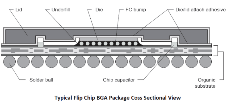
1.Typical Flip Chip BGA:The BGA package is the class of Flip Chip (FC) technology where the die is electrically connected to the PCB package substrate. The Integrated Circuit Chip is flipped or face down to make interconnection with substrate by means of solder bumps. Unlike the wire bon technology where the die was connected to substrate by means of ultrafine thin electrical wire, this FC technology inverts the chip to face downwards and make electrical connection directly with organic substrate.
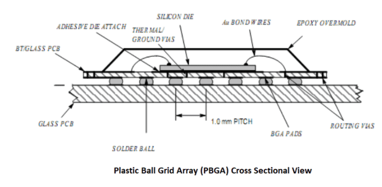
2.Plastic BGA (PBGA):As the names shows, the body package of this BGA type is plastic. It has the combination of OMPAC (over molded pad array carrier) and GTPAC (glob to pad array carrier), offering high density and cost effective solution. Normally the PBGA package ranges from 17mm x 17mm to 35mm x 35mm size/dimension and ball pitch 0.8mm to 1.0mm so that the ball count can range from 208 to 976 balls.
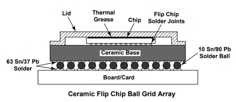
3.Ceramic BGA (CBGA):The ceramic BGAs are used in applications where high temperature is expected. The substrate base material is ceramic. They are commonly used in computer microprocessor chip technology. They use multiple layer package and the die interconnect method is “Flip Chip” not the wire bond. Coefficient of thermal expansion (CTE) for ceramic BGAs (CBGAs) is lower than that for FR-4 based PBGAs hence the stress on solder joints on CBGA package is low. The CBGA package requires more solder volume and large lands pattern to increase solder joint strength. Due to large lands, the space available for routing is less.
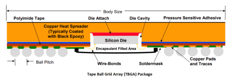
4.Tape BGA (TBGA):The TBGA package is used in the application where thinner BGA package is required. The Tape BGA (TBGA) offer less thicker version of BGA while giving optimum electrical and thermal performance. For face up, the wire bond and for face down the flip chip technology must be used. Increased thermal dissipation, excellent reliability at the PCB level, flat plane over wide temperatures and fine substrate lines and spacing unlike PBGAs wire bond.
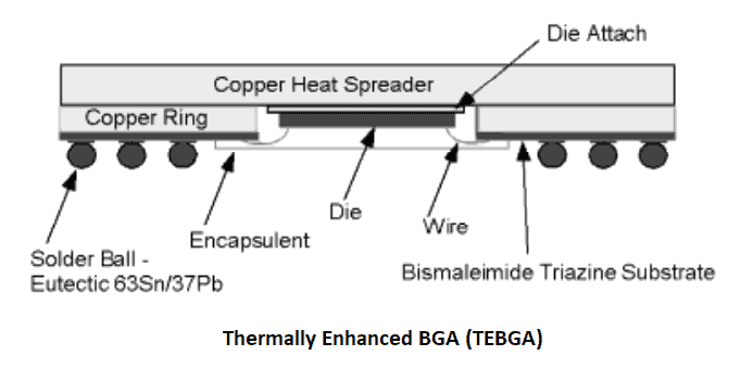
5.Thermally Enhanced BGA (TEBGA):The thermally enhanced BGA as name implies is the type of BGA with enhanced thermal feature. This is obtained by directly connecting the chip die to the copper heat spreader by means of silver filled conductive “die attach” to help dissipate heat into external heat sink. The die is encapsulated in the protective coating resin dam sealant. The die is connected to the (BT) substrate through wire bond technology.
6.Metal BGA (MBGA):The substrate base material in MBGAs is the Copper / Polyimide system, without any epoxy resin insulator. This greatly increase the electrical conduction properties of MBGA to next level. Due to the polyimide surface flatness, it is easy to implement fin pitch pattern. MBGAs are reliable and good for operating at higher frequencies above 500 MHz. The chip face down and use wire bonding technique.
7.Micro BGA:The micro BGA package uses the very fine pitch solder ball spacing. Typical micro BGA pitch size is 0.4mm however finer pitch are also coming in technology like 0.3mm and 0.25mm. But these ultrafine pitch will raise great challenge for PCB design engineer to bring routing and fanout solutions, otherwise complication in design in terms of higher layer count can raise complexity of design. The two types of land patterns used for micro-BGAs are SMD (Solder Mask Defined pads) and NSMD (Non solder mask defined pads). For routing the traces for 0.4mm pitch micro-BGA it is recommended to not place any component bigger or equal to 0201 package underneath the micro-BGA. Only use 01005 size or smaller packages for passive components for 0.4mm micro-BGA routing and component selection.
Go to the PCB ASSEMBLY GUIDELINES
Go to the PCB ASSEMBLY knowledge
PCB Blog
Contact Us
E-mail: [email protected]
E-mail: [email protected]
Skype: [email protected]
Whatsapp: +86 15012972502
Add: 2F, BUILDING H, WANDA INDUSTRIAL ZONE, ZHOUSHI ROAD, LANGXIN COMMUNITY,SHIYAN STREET, BAO 'AN DISTRICT, SHENZHEN, GUANGDONG, CHINA


 Skype Chat
 WhatsApp
  Mail inquiry