

What is the ideal RF( Radio frequency )PCB stack up?
It depends on your working frequency and target impedance. but in general rule you should avoid pushing the limits of pcb factory tolerances. for instance if you are using 50 ohm microstrips and your track width is 0.15 mm. this is not ideal because of manufacturing tolerances. at the end result this line could be a 0.12 or 0.18 mm. this is almost %20 change in width. so it's better to choose larger size than 0.5 mm tracks for micropstrips. also you should be careful about prepreg materials and resin content.other possible solution is manufacturing your pcb with impedance controlled.
When it comes to the ideal RF PCB stackup, various methods are used to PCB RF design that are microstrip, suspended strip, coplanar wave guide and grounding. You know, a microstrip consists of a fixed length of metal or wire and the under entire or part of the ground plane. Furthermore, the characteristic impedance of microstrip structure is basically from 50Ω to 75Ω.
There are some mixed laminate RF PCB Stack up for your reference.
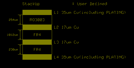
(1)4L board stack up for RO3003 + FR4 Mixed laminate RF PCB
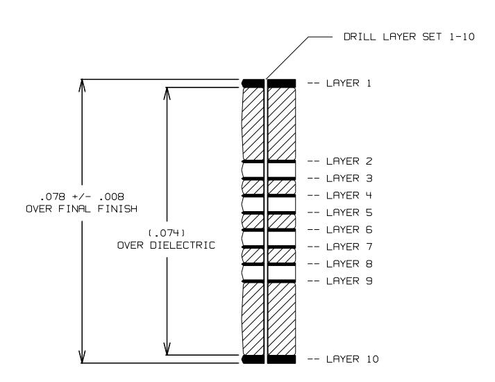
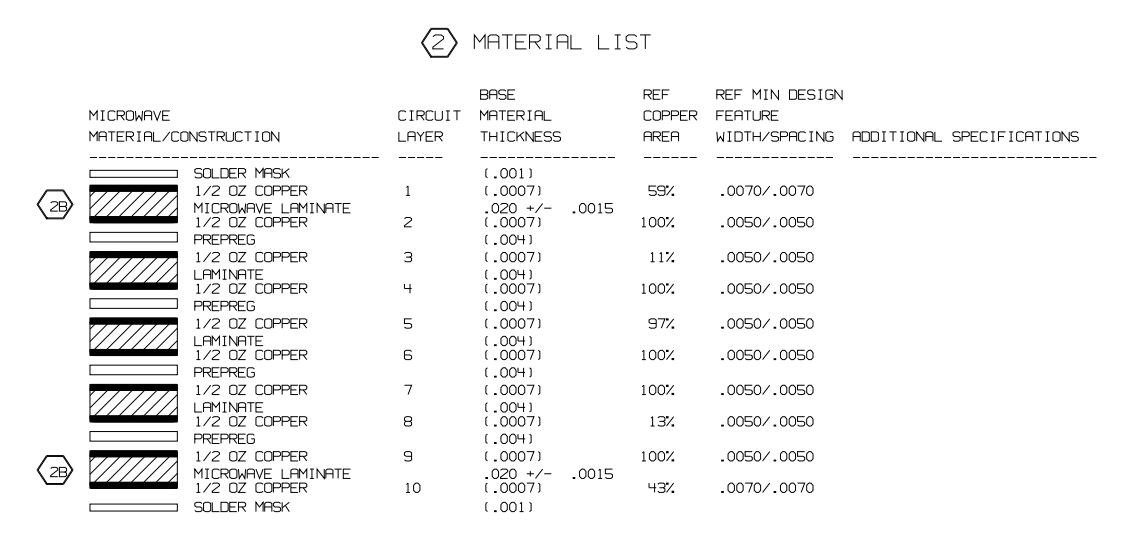
(2)10 Layer of stack up for mixed dielectric of RO4350B + FR4 RF PCB.
If any inquiry,Please send to [email protected] directly.
To know more:
what is stack up in PCB?
Introduction for Formal PCB stackups by fabricators
PCB Blog
Contact Us
E-mail: [email protected]
E-mail: [email protected]
Skype: [email protected]
Whatsapp: +86 15012972502
Add: 2F, BUILDING H, WANDA INDUSTRIAL ZONE, ZHOUSHI ROAD, LANGXIN COMMUNITY,SHIYAN STREET, BAO 'AN DISTRICT, SHENZHEN, GUANGDONG, CHINA


 Skype Chat
 WhatsApp
  Mail inquiry