

Products >> PCB manufacturing >> Metal Inlay PCB
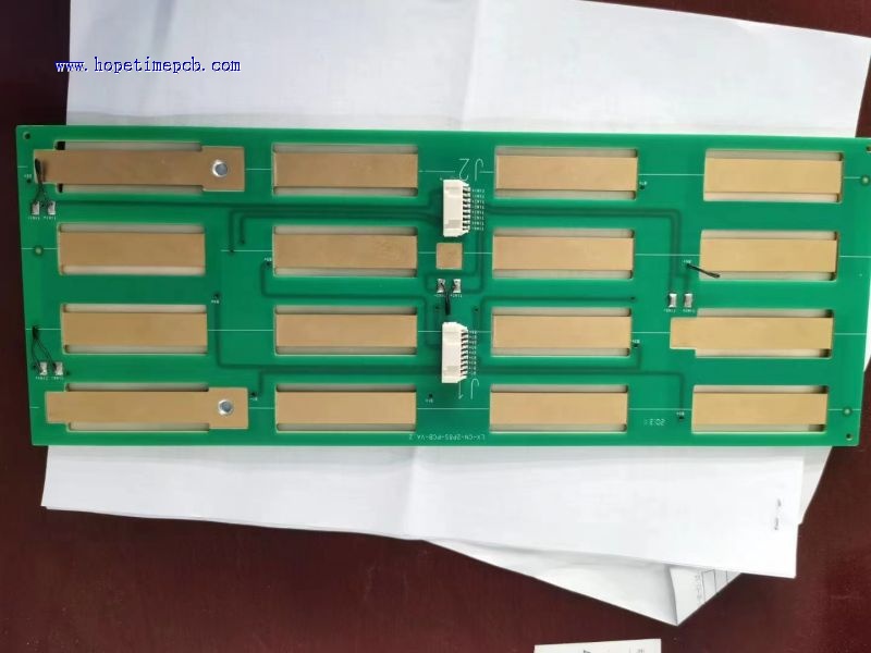
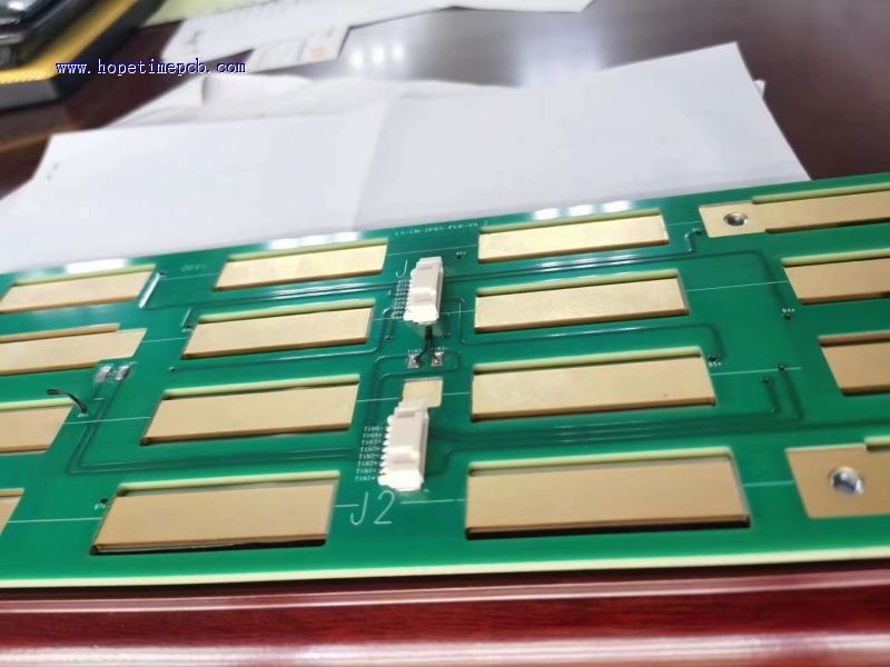
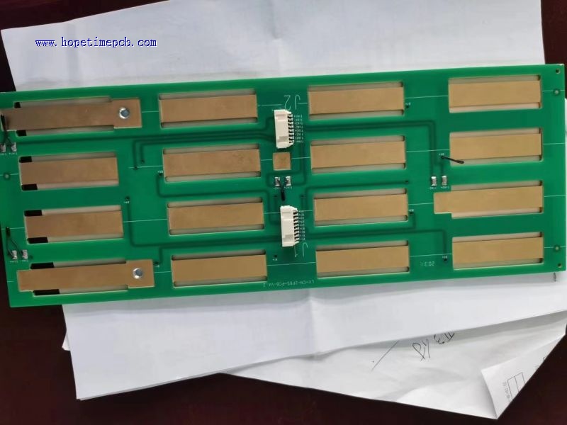
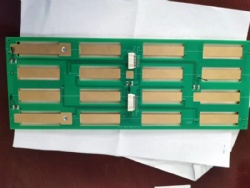
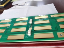
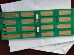
Metal Inlay PCB manufacturing special circuit board with copper inlay
- Product No.:2023821113426
- PCB board thickness:1.6mm
- Layer count:2
- PCB material:FR4
- Copper thickness:2OZ
- Surface treatment:HASL LF
- Soldermask:green
- silkscreen:White
Metal Inlay PCB manufacturing special circuit board with copper inlay
Metal Inlay PCB manufacturing
Heat from the heater elements positioned on the electronic circuit board can be released via copper inlays and directed to the heat sink bottom side by the copper inlay PCB.
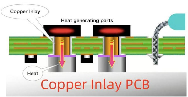
In the Metal Inlay Technology, there’s a large copper element which is pressed in the circuit board which is used to conduct heat away from the electronic components. Direct connections between this heat-emitting component and the metal inlay are possible. Typically, for this, the copper inlays used have 5mm as its minimum diameter as well as a thickness that falls between 0.8 and 2.5 mm. Depending on the size and shape, these metal inlays come either entirely or partially automated during insertion.
These metal inlays could be of any shape. Drilling or milling the circuit board creates the necessary recesses.
The initial drilling technique may generate mounting the holes to a 6.35 mm diameter, which is cost-effective. When compared to traditional thermal vias, the utilization of metal inlays significantly improves heat conductivity (via the circuit board).
Products Category
- PCB Design & Layout
- PCB manufacturing
- PCB Assembly
- BGA Assembly
- THT Assembly
- SMT Assembly
- Mixed PCB Assembly in Electronic PCBA
- Single sided PCB assembly
- Double sided PCB assembly
- Rigid-Flex Assembly
- COB Bonding Manufacturing
- Components sourcing for PCB Assembly
- SMT Stencils
- Box build assembly
- PCB engineer reverse
Contact Us
E-mail: [email protected]
E-mail: [email protected]
Skype: [email protected]
Whatsapp: +86 15012972502
Add: 2F, BUILDING H, WANDA INDUSTRIAL ZONE, ZHOUSHI ROAD, LANGXIN COMMUNITY,SHIYAN STREET, BAO 'AN DISTRICT, SHENZHEN, GUANGDONG, CHINA


 Skype Chat
 WhatsApp
  Mail inquiry