

Introduction for Base Materials for High Speed, High Frequency PCB Boards
Introduction for Base Materials for High Speed, High Frequency PCB Boards
Two questions often asked:“Will a circuit board made of FR4 laminate work for my High Speed or High Frequency design?” and, “If FR4 isn’t OK, where do I turn?”
Answer:these questions are specific to each individual circuit and can only be answered through analysis of the characteristics of FR4 verses other material choices,relative to the demands of the circuit’s noise budget.
1.Circuit Types – There are two basic types of circuits
--High frequency, RF /Analog (aka- RF/Microwave)
--High Speed digital
RF/Analog circuits usually process precision and/or low level signals. Hence these circuits require much tighter control of parameters pertaining to signal losses. The two losses of greatest concern are losses caused by signal reflections, due to impedance mismatch or impedance changes and the loss of signal energy into the dielectric of the material. Some critical applications also need to focus on losses due to ‘Skin Effect’.
Impedance variations result from two things, material parameters that vary with changes in frequency or temperature and variations in the processes at the fabricator. The amount of signal lost into the dielectric is a function of the material’s characteristics. Skin effect can be partially controlled through choice of copper type in or on the PCB board.
Material choice can have a major impact on all these sources of energy loss. As a result materials geared to the RF/Analog domain tightly control parameters such as Dielectric Thickness, Dielectric Constant (εr/Er/DK), Loss Tangent (tan (δ)) and even copper type.
In contrast digital circuits can tolerate much greater signal loss and still function. Losses are important in the digital domain as well but because of very broad noise margins of digital ICs, usually don’t affect circuit performance until they become a very significant portion of the noise budget. This most often occurs at very high operating frequencies.
Also digital circuits are generally very complex and dense and often require very large,high layer count boards. This tends to put the emphasis for digital materials on process capabilities and cost. These needs have spawned the second group of materials, geared to digital applications.
2.PCB Materials Development –
Through the several decades prior to the 1990’s many high end laminates were developed for use in RF/Analog circuits, mostly for military applications. Most of these materials are expensive and only a few work well for multilayer boards. Fortunately most of the RF/Analog circuits for which they were developed have low complexity and generally don’t require high layer count boards. During that same period virtually all digital circuits and most low frequency analog circuits utilized the spectrum of FR4 base materials.
Through the 1990’s and into this century we have seen a shift in the focus of high frequency and high speed circuitry. As the commercial end of the RF/analog industry has dramatically increased in size, attention has been sharply drawn to the need to produce high end RF/Analog laminates without the ‘high end’ price tag.
At the same time many digital circuits for telecomm equipment and computers are being pushed into the realm of frequencies where losses can be significant. In today’s sub-one nanosecond rise time digital circuits, where clock frequencies are in the hundreds of MHz, the selection of base materials and prepregs used in the laminate structure can play a role in the success or failure of the overall system performance.
3.Material Parameters –
There are a number of material parameters and characteristics important to the overall success of any circuit board. There are 4 main parameters that generally affect signal losses,
A:Er
Relative permittivity is a measure of the effect an insulating material has on the capacitance of a conductor embedded in the material or surrounded by it. It is also a measure of the degree to which an electromagnetic wave is slowed down as it travels through the insulating material. The higher the relative permittivity, the slower a signal travels on a trace, the lower the impedance of a given trace geometry and the larger the stray capacitance along a transmission line. Given a choice, lower dielectric constant is nearly always better.
Relative permittivity varies with frequency in all materials. In some materials the variation is small enough that it can be ignored even in very sensitive applications. Some materials, like FR4, have broad variations in Er with changes in frequency.
Changes in Er can be a serious problem in broadband analog circuits. Two common problems are changes in transmission line impedance and changes in signal velocity as the circuit operates across its entire frequency range. Impedance changes cause reflections of signal energy that affect circuit performance and often create circuit malfunction. Changes in signal velocity will result in phase distortion. Broadband RF and microwave circuits usually need to be fabricated from materials with low and fairly constant Er.
Changes in Er with frequency can also affect digital circuits. The greatest effect is to cause errors between calculated and measured impedance. Most suppliers of FR4 laminate measure Er at 1 MHz. If impedance is calculated using an Er measured at 1MHz and the resulting circuit board’s impedance is measured using a TDR with rise time set somewhere between 50 and 150 psec, the resulting impedance measurement will be different than the calculated impedance by as much as 5 to 6%.
Engineers and designers need to determine correct values of Er for the board material, at operating frequency. With that knowledge impedance calculations can be made using Er at the frequency of operation and at the test frequency so the effects can be compensated for and problems won’t develop.
Another area involving Er that can have major impact is an ultra-fast switching application where low Er is necessary to ensure rapid propagation of signals. In these situations,be they analog or digital, materials must be selected that offer the operating characteristics required. There are a number of materials designed for analog circuits with low and stable Er. There are also several materials designed for the digital arena that offer a fairly low and stable Er.
Another potential concern for sensitive analog circuits is the ‘Coefficient of Thermal Expansion relative to Permittivity’ (CTEr). If the circuit will operate in a broad temperature changing environment attention may need to be paid to CTEr.
B&C:Dielectric Thickness and Trace Width-
Both of these parameters play a key role in transmission line impedance. Control of each is necessary during fabrication of the board, with the greatest degree of control needed for high frequency analog circuits.How much these parameters vary is a function of both process control by the fabricator and selection of the base material.
A 20% change in dielectric thickness (trace height above the power or ground plane) can cause as much as a 12% change in impedance (Zo). As dielectric thickness increases, Zo increases. This becomes especially critical with very thin dielectric layers. Due to resin type, glass or filler type and glass/filler-to-resin ratios, some materials are much easier to maintain control of dielectric thickness than others. A tolerance on dielectric thickness is generally listed on the data sheets or in the specifications for the various materials.
A 20% change in trace width can cause as much as a 10% change in impedance. As width increases, Zo decreases. Control of trace width is both a function of process control by the board fabricator and to some degree the type of copper used on the base material.
Printed circuit copper comes in two forms, rolled sheets and electrodeposited (ED) sheets. Each has advantages and disadvantages. The contribution each makes to skin effect is discussed later.
Rolled copper is made by cold forming, with heavy steel rollers, thick copper sheets into sheets thin enough to use on a PC board. Rolled copper has mechanical stresses built into it by the rolling process and excellent flatness on both surfaces. This flatness coupled with the high mechanical stresses cause rolled copper to be more prone to delaminate than ED copper, from the base resin. The advantage of the high density and flat surfaces of rolled copper is better control of etching, hence very tight control of trace width.
Electrodeposited (ED) copper is formed by turning a metal drum in a solution of copper sulfate. The copper/liquid is contained in a tank called a plating cell. As the negatively charged drum rotates through the solution in the positively charged cell, copper migrates to the drum surface and forms as an even copper deposition.
At the top of the rotation, the copper is pulled off the drum as a foil sheet. The thickness of the copper is a function of charge potential between the cell & drum and the speed of the drum.
ED copper has no internal stresses. Additionally it has one smooth surface (the drum surface) and one surface filled with little, spiked bumps known as dendrites. The rough,low density and no stress nature of ED copper (compared to rolled copper) makes it less prone to delaminate but also makes it more difficult to etch precisely.
The effect on impedance, caused by the difference in etch capability between rolled and ED copper, would barely be noticed in a typical digital circuit. The difference can be significant in an analog circuit needing precise impedance control. The current spectrum of materials designed for digital applications are all supplied with ED copper. Among the spectrum of analog based materials, most offer rolled or ED copper.
Copper thickness plays a minor role in the impedance of a transmission line. A 20% change in copper thickness will cause only a 3% change in Zo. This secondary effect,coupled with the ability of laminate suppliers and fabricators to control copper thickness,make it a variable we can generally ignore. In a sensitive, ultra high frequency analog circuit copper thickness variations can have a noticeable effect, but circuits demanding such ultra tight control of copper thickness are rare.
Copper choice vs resin material is listed on the data sheets or in the specifications for various materials.
Material selection will play a role in trace width control and a key role in dielectric thickness control but the fabricator is also a major contributor to proper control of both,especially in high layer count boards. Fabricator selection is an issue that’s frequently not given just attention. All too often the purchasing department of many OEMs and contract assembly houses will make a blind selection of the fabricator based solely on price and delivery. Given the complex nature of quality board fabrication, that’s a really bad idea, even in the digital domain. In the high frequency analog domain it’s nearly a criminal act. But perhaps that’s the subject of another article.
D:Loss Tangent.
Loss tangent is a measure of how much of the signal pulse (electromagnetic wave) propagating down the PCB transmission line will be lost in the dielectric region (insulating material between copper layers). Loss tangent is a function of the material’s resin type and molecular structure (molecular orientation).
Lower loss tangent equates to more of the output signal getting to its destination(s). The loss factor becomes especially important when working with low level signals like those in many receivers and block down converters (LNB’s) or with very high power applications, where a 5% difference in signal loss could mean many watts of lost energy.Also of significance in the digital domain are multi-gigabit signals, such as those in ultra high speed Ethernet circuits.
Ideally we want to specify and use materials with very low loss tangent. Unfortunately that can carry a heavy cost penalty, which is why we need to analyze which materials will work and which won’t. This gives the freedom to choose a cost effective solution.
The amount of signal loss in a circuit is not only a function of material type but is also a function of frequency and line length in or on the PCB. Length will be discussed.Frequency must be viewed differently in digital circuits than in analog circuits. Analog signals consist of sine waves and variations of sine waves and what you see in the time domain is basically what you get in the frequency domain.
When a sine wave is launched into a transmission line, the frequency of the sine wave propagates unchanged but the amplitude will drop off due to the effects of loss tangent.Since analog signals are sine wave in nature, loss tangent causes a reduction in signal amplitude as the signals propagate. The further a signal travels the greater the reduction in amplitude.
In contrast digital signals are square waves, which consist of a series of embedded sine waves called harmonics. These harmonics are multiples of the clock frequency and generally have strong amplitude out to a frequency that can be determined by equation 1.
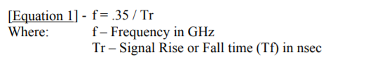
This means that digital signals have a bandwidth of frequencies that are affected by Loss Tangent. The bandwidth starts at the clock frequency of the circuit and extends to the frequency determined by equation 1. As an example, a circuit with 200 psec rise time signals and a clock frequency of 500 MHz will have a bandwidth of concern from 500MHz to 1.75 GHz.
When a digital signal propagates through a transmission line, each of the sine wave harmonics in the rising and falling edge lose amplitude, as the signal propagates, due to loss tangent, with the highest frequency harmonics suffering the highest losses. The loss of amplitude of the harmonics is manifested as a degradation of Rise and Fall time of the signal. This can seriously affect timing of level sensitive signals and can affect both timing and circuit performance of edge driven signals (clocks, enables, resets, etc.).
There is certainly no rule of thumb to decide at what point an analog circuit will be affected by losses. Every analog circuit must be analyzed to determine anticipated loss verses acceptable loss.
Digital circuits must also be analyzed individually, but in general when losses to the first harmonic exceed approximately 3dB across the total length of the transmission line it can be assumed that circuit performance will be severely affected. That is to say in a 10 inch line, the amount of loss per inch shouldn’t be allowed to exceed 0.3 dB. Again, this is a rule of thumb and is not always a safe bet but it’s a good estimation of roughly when to be concerned.
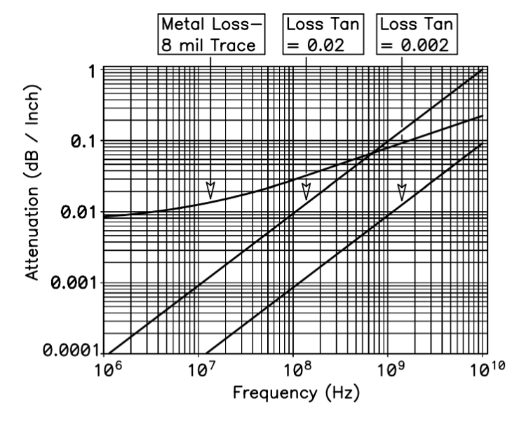
Figure 1 – Graph of Attenuation (tan(δ) & Skin Effect) verses Frequency
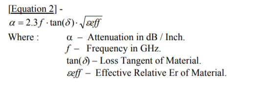
The graph in figure 1 can be used to determine the actual amount of loss per inch in materials with a tan(δ) of .02 (typical for FR4) and materials with a tan(δ) of .002(typical for several Teflon (PTFE) based materials). Equation 2 was used to build the graphs in Figure 1 and can be used to calculate tan losses for other materials. Notice the graph also shows attenuation for resistive loss in the metal (next section).
There is also a fifth issue that can cause significant losses at some frequencies, Skin Effect. To gain true control of high speed and high frequency signals, all of these must be considered.
E&F:Resistive Losses and Skin Effect –
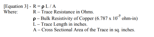
Voltage drop along a PCB trace, due to resistance in the trace, is a fact of life. From DC through frequencies up to a few MHz, the current in a trace moves through the entire cross sectional area of the trace. At these frequencies resistance is extremely small, hence resistive losses are extremely small. An 8 mil wide trace, at low frequencies, made of 1 ounce copper (1.4 mil) has an approximate resistance of .06 ohms per inch. This was derived from equation 3.
When driving a signal into a 50 ohm line with a 50 ohm load, it’s easy to see that the resistive drop at these frequencies would be extremely small, in the order of a few milivolts.As frequency increases the energy moving in the trace is forced to the outer perimeter by the large magnetic fields present in higher frequency signals. This is known as skin effect because the majority of the energy is forced to the outer skin of the trace.
Penetration of the signal into the trace is measured in ‘Skin Depths’, with approximately 66% of the energy penetrating to one skin depth and approximately 97% of the energy penetrating to three skins depths.One skin depth at 10 MHz is .0008 inches. At 10 GHz one skin depth is .000028 inches.Looking at the example of 10 GHz, most of the energy in the trace would be limited to a depth of approximately 84 millionths of an inch. The net result is a decrease in effective cross sectional area of the trace because much of the copper is not used. It’s as if the trace were hollow.
Because of skin effect, resistance of an 8 mil trace at 10 GHz will be a little more than 1 ohm per inch. That means the resistive drop from a 3.3 volt signal in a 5 inch, 50 ohm line with a 50 ohm load, at 10 GHz will be greater than 300 mv. In most cases this cannot be ignored.
What effect does this have on material choice? In the digital domain, none. Among the materials available for analog boards, as mentioned earlier, some are available with rolled copper. Because of the smooth, dense nature of rolled copper is will suffer less from skin effect losses than its much rougher counterpart, ED copper. According to data gathered by laminate suppliers of high frequency materials, the losses in ED copper are about 12% higher than rolled copper losses, from 3 to 12 GHz.
Those needing to calculate skin effect are encouraged to visit Howard Johnson’s web article, “Skin Effect Calculations” (see references). Howard does a great job of walking through the calculation of skin depth and resistance at high frequencies. Howard’s calculations assume ED copper. When using materials with rolled copper, losses can be adjusted according.
At high frequencies, on microstrip traces (referenced to one plane only), almost all the energy will be on the side of the trace nearest the plane. On stripline (referenced to two planes) the energy will balance for centered stripline and will be offset proportionally in off centered stripline. This is called ‘Proximity Effect’. As a result, other than in centered stipline, changes in copper weight (trace thickness) will have little effect on trace resistance at high frequencies. In all cases, changes in width and length will have the greatest effect on resistance at high frequencies.
G&H:Combined Effect of Loss Tangent and Skin Effect –
In digital circuits resistive drops will have an effect similar to that of loss tangent, meaning rise and fall time of the wave will degrade due to decreased amplitude of the harmonics, with the highest frequency harmonics being affected the most. In analog circuits the effect is usually a direct loss of signal amplitude.
Looking at the curve for metal loss in figure 1, we can see that above 1 GHz loss tangent becomes much more severe than skin effect in FR4. To get a true picture of signal loss we need to calculate the combined effects of loss tangent and skin effect.
Studies performed by groups such as AMP (Tyco) and NESA (see references) indicate the combined effects of loss tangent and skin effect are often not severe enough, with digital circuits in FR4, to cause circuit malfunction, well into the low GHz operating range.The studies also show that changing material will improve signal quality. But if a circuit will function at a given frequency in a given material, switching to a better grade material at a higher price may offer no benefit. Each circuit should be analyzed based on its particular requirements and available noise and timing budget, especially in the analog domain.
4.Material Choices –
As mentioned, materials are basically divided into two groups, those designed for digital circuits and those designed for analog circuits. Based on operating parameters, the major differences between the materials are –
1) Analog materials generally have a much lower Er that’s more stable over frequency and changing temperature.
2) Analog materials generally have tighter tolerance on dielectric thickness.
3) Analog materials are often offered with Rolled or ED copper. Digital materials come with ED copper only.
4) Only a few analog materials are designed for multilayer applications. All digital materials are designed for multilayer applications.
5) Loss tangent varies a great deal across the material choices, but is generally much lower in analog materials, often by a factor of 10 or more.
Some of the materials aimed at the digital arena could be used in an analog circuit and in many cases that might be a good use of resources. In fact many of the materials now considered to be high end digital materials were developed for the commercial end of the high frequency analog arena. Looking through the specs of these materials it will be apparent which are well suited to analog applications, even at very high frequencies.
Table 1 lists materials for digital boards. Some materials list a broad range for Er.Within a given material low glass content yields a low Er and high glass content yields a higher Er.
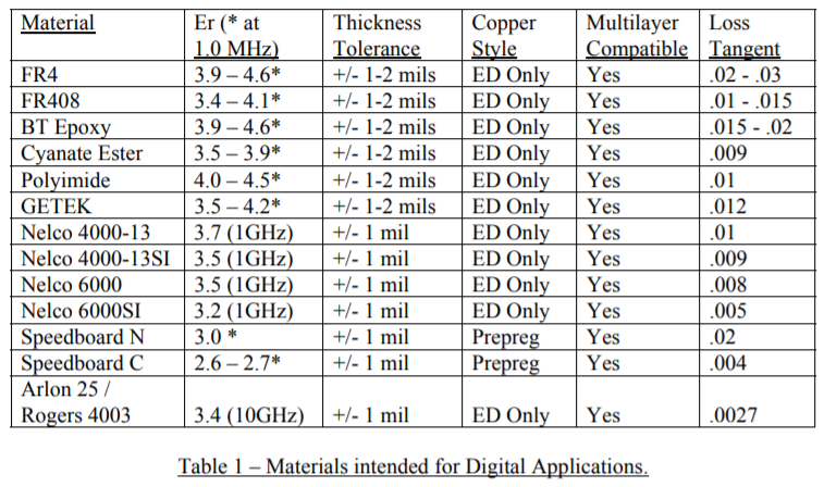
Of the materials listed above BT Epoxy, Cyanate Ester and Polyimide were developed as replacements for FR4 in applications needing extreme mechanical stability, with Cyanate Ester also offering some improvement in performance. GETEK and FR408 are intended to offer improved electrical performance. The four Nelco materials offer a great deal of improvement in electrical performance and the two Speedboard materials were designed as prepregs, to use in applications where a low Er material can be mixed with fairly low cost materials to create a board with a lower Er and imprved performance.
Arlon 25 and Rogers 4003 were originally designed to fit into the analog market as a commercial replacement for some of the high cost, high end military grade laminates.They are listed with the digital materials because many engineers consider them an excellent choice when very high end parameters are required in digital circuits.
Table 2 lists materials for analog circuits. The materials listed give an order number for Rogers Corp only. This is not an attempt to push one supplier. The numbers listed are most familiar to the writer. Most of these materials have equivalent choices from other makers of laminates (Arlon. Taconic and 3M – See supplier list at end of article)
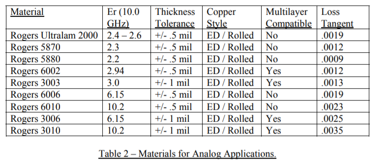
The Ultralam and the 5000 and 6000 series materials are all approved for military applications. The 3000 series materials are commercial equivalents of the 6000 series materials. Each of these is designed for specific environments and applications, all of which are too lengthy to state in this article. Research of the materials and their equivalents from other suppliers is encouraged. As mentioned, most of these materials have an equivalent from suppliers such as Arlon, Taconic or 3M.
Material costs are not listed, as they change frequently. The user is strongly encouraged to talk with their fabricator about cost of the finished board, utilizing one material verses another. Some of the fairly expensive materials are easy to fabricate and might result in a finished board that’s less expensive than a cheaper material that creates manufacturing difficulties. Overall costs of the material alone range from $1.50/sq. ft., for the low end of the FR4 spectrum, to as much as $100.00/sq. ft, for some of the very high end, analog laminates.
Tg – One material parameter not discussed is Tg. All materials exhibit changing temperature coefficients of expansion as temperature increases. Tg is the temperature at which materials begin to expand at an uncontrolled rate. Boards operating beyond Tg are subject to failure. This is another parameter the reader is encouraged to understand.
For circuits operating in a broad temperature environment, additional parameters that should be investigated are CTEr, CTE and CTE of the base material verses copper.
Conclusion – The reader is encouraged to run through the equations provided for Loss Tangent and check those available on Howard Johnson’s website for Skin Effect, then compare the numbers against the available noise and timing budget for the circuit in question. This analysis will show that most digital circuits today (0.2 to 2.0 nsec rise and fall times) can use FR4 as a base material without concern of circuit malfunction.
Analog circuits must always be analyzed to compare the operating parameters of the material against the acceptable losses in the circuit, then choose the material most suited to the application, looking at cost as only one of the driving factors.
Once a material is chosen, equal care should go into selection of the fabricator for the bare board, keeping in mind that an acceptable level of quality and lowest price may not walk hand in hand. This is especially true for sensitive, high frequency analog boards,requiring fabricators who have the equipment and process controls needed to make boards from the specialized materials discussed. Remember too, fabricators can be a wealth of knowledge about materials.
Article written By: Rick Hartley, March 2002, Published in PCB & A
PCB Blog
Contact Us
E-mail: [email protected]
E-mail: [email protected]
Skype: [email protected]
Whatsapp: +86 15012972502
Add: 2F, BUILDING H, WANDA INDUSTRIAL ZONE, ZHOUSHI ROAD, LANGXIN COMMUNITY,SHIYAN STREET, BAO 'AN DISTRICT, SHENZHEN, GUANGDONG, CHINA


 Skype Chat
 WhatsApp
  Mail inquiry