

Guidelines for RF & microwave PCB Design
Guidelines for RF & microwave PCB Design
Today RF circuitry is crammed into a large variety of commercial products. Most of these are handheld wireless devices for medical, industrial, and communications applications, plus applications in a variety of fields are migrating from desktop models to become portable communications units. Not only is RF becoming more ubiquitous, but microwave circuitry as well, both capturing very high frequencies (VHF) and ultra-high frequencies (UHF).
PCBs now encompass much more than pure digital or mixed-signal technologies, and the PCB layout designer faces many more challenges when designing sub-assemblies with high frequency RF and microwave.
--The RF frequency range is typically from 500 MHz to 2 GHz, and designs above 100 MHz are considered RF.
--The microwave frequency range is anything above 2 GHz.
There’s a considerable difference between RF and microwave circuits versus typical digital and analog circuits. In essence, RF signals are very high frequency analog signals. Therefore, unlike digital, at any point in time an RF signal can be at any voltage and current level between minimum and maximum limits.
Standard analog signals are assumed to be between DC and a few hundred megahertz. But RF and microwave signals are one frequency or a band of frequencies on a very high frequency carrier (Figure 1 ).
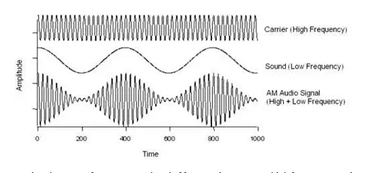
Figure 1: RF and microwave signals are one frequency or a band of frequencies on a very high frequency carrier.
Unlike digital signals associated with one voltage or one current, RF and microwave signals operate on a frequency.
RF and microwave circuits are designed to pass signals within a certain band. They use band pass filters to transmit signals in a so-called band of interest. The signal within a range of frequency passes through this band range, and the rest of the frequencies of the signal are filtered. A single band can be very narrow or very wide and carried upon a very high frequency carrier wave.
Issues with PCB design and RF/microwave
For the most part, PCB layouts that include RF and/or microwave circuits are difficult to design. However, regardless of their difficulty, the rule of thumb is to start with the basics and follow the laws of physics. Up front, the PCB designer needs to understand that microwave signals are highly sensitive to noise. The possibility of incurring ringing and reflections must be treated with great care.
When working with very high-speed digital signals in the gigahertz range or 10Gb per second, for example, the PCB designer has to follow certain guidelines and rules. When RF and microwave enter the layout, the PCB designer must have the same mindset, yet multiply that mindset many times simply because RF is far more sensitive than very high-speed digital signals.
1.Impedance matching
impedance matching is extremely critical for RF. Digital signals — even if they are very high-speed — have a certain tolerance. But for RF and microwave, the higher the frequency, the smaller the tolerance becomes. For example, the PCB designer must keep it at 50 ohms — 50 ohms out from the driver, 50 ohms during transmission, and 50 ohms into the receiver.
2.Return loss
the return loss must be minimized. This loss is caused by signal reflection, or ringing. The return is the path taken by the return current (Figure 2) .
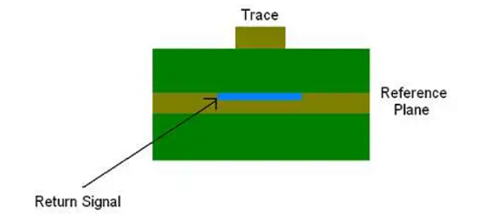
For example, take a single-ended signal going from the driver to the receiver. Obviously, there has to be a return signal from the receiver to the driver. If it’s a single-ended signal, then the return typically takes the path of least impedance.
At very high microwave frequencies, the return signal takes the path of least inductance. Ground planes underneath the signals are good at providing this path. Therefore, there should be no discontinuities in the plane underneath the signal all the way from the driver to the receiver. However, If there is a cut in the ground or the ground plane doesn’t exist underneath that trace, the signal will still somehow find its way to the driver. It will go through power planes, through a PCB’s multi-layers or through some other route – it will definitely find a return path. But such a path won’t be ideal, and thus will cause reflection and ringing since it will no longer be an impedance controlled signal (Figure 3 ).
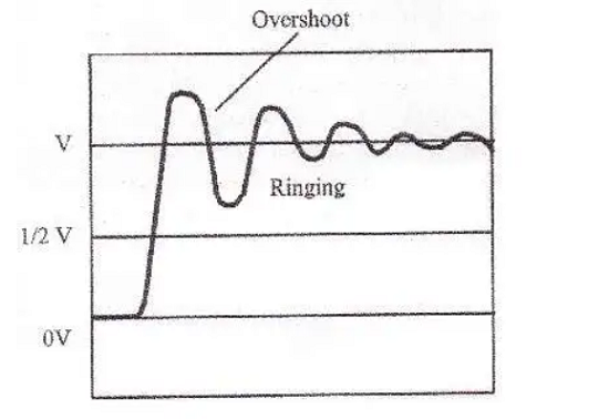
Figure 3: Ringing created by impedance mismatch on a transmission line
3.crosstalk
The PCB designer must also keep the crosstalk factor in mind whendesigning RF and microwave circuits. As the system performance and board densities increase, the problem of cross talk and how to deal with it becomes more important. Cross talk is the transfer of energy between adjacent conductors due to mutual inductance and shunt capacitance. The coupled energy from the active line is super imposed on the victim line.
The coupled signals that flow toward the receiver constitutes forward crosstalk. Those traveling toward the source constitute backward crosstalk.Backward crosstalk is the sum of the inductive and capacitive coupling, whereas forward crosstalk is the difference between the two.Crosstalk is a major issue in high frequency designs. This is because it is directly proportional to the edge rates of the active line.
4.the proximity of the two lines and the distance
Other factors are the proximity of the two lines and the distance over which the two lines run parallel to each other. Hence, the high speed signals should be routed as far apart as possible. Ideally the distance from center to center should at least be four times the trace width for these signals.The distance that the lines run parallel to each other should also be kept to a minimum. Other solutions include reducing the dielectric spacing between the line and its reference plane or introducing a co-planar structure, where a ground plane is inserted between the traces. Terminating the line on its characteristic impedancecan also reduce the cross talk by as much as 50 percent.
5.impedance controlled
All traces on the PCB do not need to be impedance controlled. Only if the total length of the trace from the driver to the receiver is greater than 1/16th of the wavelength of the signal, then impedance control of that trace is required. 1/16th of the wavelength is called the critical length of the signal.Frequency is inversely proportional to wavelength. The higher the frequency, the shorter the wavelength becomes. For example, for 1GHz on a microstrip FR4-based PCB, the critical length is approximately 0.425 inches. Therefore, if you are routing a 1GHz signal its total length is greater than 425 mils, then that trace needs to be impedance controlled. The critical length is also dependent on the material of the PCB as well as the transmission line technologies.
6.laminate properties
When using RF circuits, the designer needs toconsider the laminate properties, such as the dissipation factor anddielectric constant (Dk) value and its variation. FR4 has a higherdissipation factor than high frequency laminates like Rogers and Nelco.This means that insertion losses are much higher when using FR4. Theselosses are also a function of frequency and will increase as frequencyrises. Secondly, the Dk value of FR4 can vary as much as 10%. This inturn varies the impedance. High frequency laminates have more stablefrequency properties.
Then there is the Dk value itself. When itcomes to microwave circuits, the Dk value is tied to the size of thecircuit elements, so the designer may be able to decrease the size ofthe circuit by choosing a laminate with a higher Dk value.
7.Avoid losses
Asstated above, impedance mismatching results in reflections. If a traceis not properly terminated or if the return path is not optimized, then there will be reflection or ringing on the signal. There are othersignal losses as well. The first one is the skin effect loss of asignal, specifically the skin effect loss on the trace of a signal. It’simportant to note that skin effect is a measure of frequency.
At high frequencies, electrons tend to flow on the outer surfaces of the conductor; this is what is known as “skin effect.” On the trace itself,there is an extremely small area that is used as a funnel to move electrons. This funnel causes heat on the trace, and some of that energy going through the trace is converted to heat and lost, thus creating the skin effect loss of a signal.
Dielectric loss is a companion to skin effect loss since both can be created at extremely high frequencies. Like the skin effect loss, dielectric loss is created when electrons flow through a conductor. There is quiet energy in those electrons. They bounce back and forth with the electrons on the FR4 PCB substrate, for example. During this interaction, some of the energy from the electrons flowing through a conductor is then transferred to the electrons on the FR4. Consequently, that energy is converted to heat and subsequently lost, and dielectric loss is created. Figure 4 shows losses in a PCB transmission line as a function of frequency.
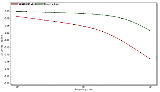
Figure 4: Losses in a PCB transmission line
In such instances, for extremely high frequency microwave circuits it’sbest to use polytetrafluoroethylene Teflon, known in the industry as PTFE material. These laminates have a dissipation factor of around 0.001(compared to FR4’s dissipation factor of 0.02). Secondly, using goldbody on RF circuits can greatly reduce the skin losses.
To know more:
The basic knowledge about RF Microwave PCB design
PCB Blog
Contact Us
E-mail: [email protected]
E-mail: [email protected]
Skype: [email protected]
Whatsapp: +86 15012972502
Add: 2F, BUILDING H, WANDA INDUSTRIAL ZONE, ZHOUSHI ROAD, LANGXIN COMMUNITY,SHIYAN STREET, BAO 'AN DISTRICT, SHENZHEN, GUANGDONG, CHINA


 Skype Chat
 WhatsApp
  Mail inquiry