

What is the PCB soldermask opening?
What is the PCB soldermask opening?
Solder Mask opening: The place where there is no solder mask is called the solder mask opening.
The circuit on the PCB are covered with soldermask to prevent short circuits and damage the device. The so-called soldermask opening is to remove the paint layer on the circuit, so that the circuit can be exposed to tin.On PCB, a soldermask is usually put on most professionally made boards.It is an extra step and applied to the nearly finsihed board stack up, one for the top and one for the bottom if a 2 or more multilayer board.
Most photomasks are called a liquid photoimiageable mask and are designed as an artwork image like all the trace layers using the PCB design software.
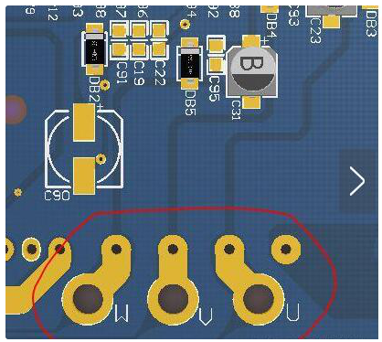
The mask is tough, it withstands soldering without damage and when placed over metal traces keeps any solder from sticking to those places.So to get solder in the right places, openings are placed in the soldermask artwork where no soldermask is applied. Typically these are solder pads for thru-hole components, solder pads for surface mount components, mechanical mounting pads where a ground connection has to be made, contacts for mounted contacts that directly contact board etch pads for continuity, etc. Solder mask is left between pads and over all the exposed traces to prevent solder shorts from solder bridges and splashes. Usually the soldermask opening will be about 3 mils (.003″) larger than the solder pad that is exposed.They also provide protection against shorts in operation by metallic junk.
The students who have removed the computer know that the memory stick has a gold finger, as shown below:
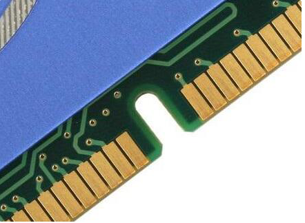
The golden finger here is to opening, plug and play.There is also a very common function of opening the opening, which is to increase the thickness of the copper foil in the later period, which is convenient for excessive current, which is more common in the power board and the motor control board.
Go to the PCB knowledge Page
Go to the PCB design resources page
Back to the technology data
PCB Blog
Contact Us
E-mail: [email protected]
E-mail: [email protected]
Skype: [email protected]
Whatsapp: +86 15012972502
Add: 2F, BUILDING H, WANDA INDUSTRIAL ZONE, ZHOUSHI ROAD, LANGXIN COMMUNITY,SHIYAN STREET, BAO 'AN DISTRICT, SHENZHEN, GUANGDONG, CHINA


 Skype Chat
 WhatsApp
  Mail inquiry